CS5520-BSZ Ver la hoja de datos (PDF) - Cirrus Logic
Número de pieza
componentes Descripción
Lista de partido
CS5520-BSZ Datasheet PDF : 41 Pages
| |||
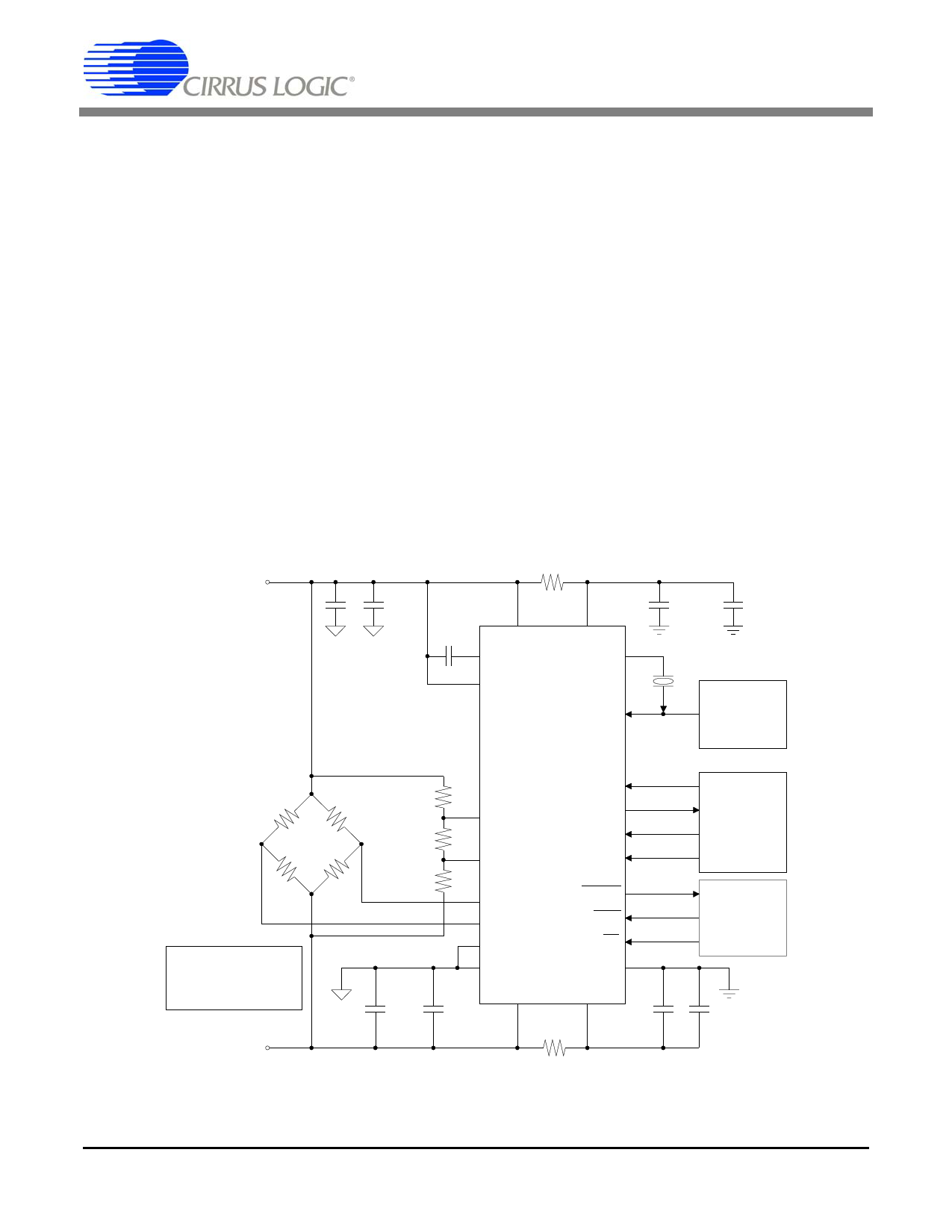
CS5516, CS5520
THEORY OF OPERATION
The front page of this data sheet illustrates the
block diagram of the CS5516 and CS5520 A/D
converter. The device includes an instrumenta-
tion amplifier with a fixed gain of 25. This
chopper-stabilized instrumentation amplifier is
followed by a programmable gain stage with
gain settings of 1, 2, 4, and 8. The sensitivity of
the input is a function of the programmable gain
setting and of the reference voltage connected
between the VREF+ and VREF- pins of the de-
vice. The full scale of the converter is VREF/( G
x 25) in unipolar, or ±VREF/(G x 25) in bipolar,
where VREF is the reference voltage between
the VREF+ and VREF- pins, G is the gain set-
ting of the programmable gain amplifier, and 25
is the gain of the instrumentation amplifier.
After the programmable gain block, the output
of a 4-bit DAC is combined with the input sig-
nal. The DAC can be used to add or subtract
offset from the analog input signal. Offsets as
large as ±200 % of full scale can be trimmed
from the input signal.
The CS5516 and CS5520 are optimized to per-
form ratiometric measurement of bridge-type
transducers. The devices support dc bridge exci-
tation or two modes of ac (switched dc) bridge
excitation. In the switched-dc modes of opera-
tion the converter fully demodulates both the
reference voltage and the analog input signal
from the bridge.
+5V
Analog
Supply
-
Unused logic inputs
must be connected
to DGND or VD+
-5V
Analog
Supply
10 Ω
1 µF 0.1 µF
0.1 µF 1 µF
1 µF
2
1
3
VA+
MDRV-
MDRV+
20
VD+
XOUT 23
XIN 22
CS5516
CS5520
SCLK 16
18
9 VREF+
SOD
SID 17
+
10 VREF-
SMODE 24
Optional
Clock
Source
Serial
Data
Interface
6 AIN+
7 AIN-
5 AGND1
8 AGND2
DRDY 15
RST 13
CS 14
DGND 19
Control
Logic
0.1 µF 1 µF
VA-
VD-
4
21
10 Ω
1 µF
0.1 µF
Figure 2. System Connection Diagram: DC Excitation Mode (EXC bit = 0), F1 = F0 = 0.
DS74F21
11
Share Link: 