CS5520 Ver la hoja de datos (PDF) - Cirrus Logic
Número de pieza
componentes Descripción
Lista de partido
CS5520 Datasheet PDF : 41 Pages
| |||
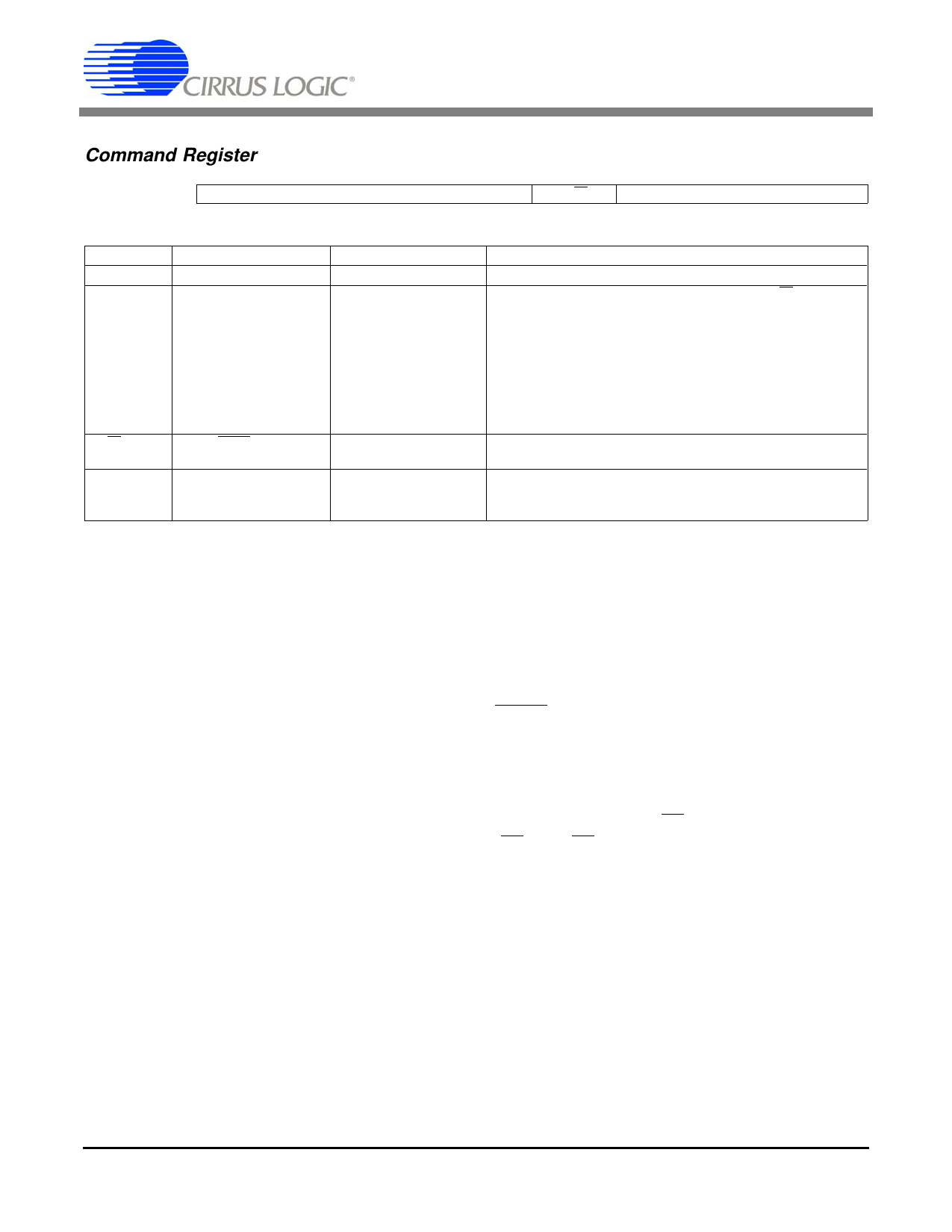
Command Register
D7
D6
D5
D4
D3
1
RSB2
RSB1
RSB0
R/W
CS5516, CS5520
D2
D1
D0
0
0
0
BIT
D7
RSB2-0
NAME
D7
Register Select Bit
R/W
Read/Write
D2
D2
D1
D1
D0
D0
VALUE
1
000
001
010
011
100
101
110
111
0
1
0
0
0
FUNCTION
Must always be logic 1
Selects Register to be Read or Written per R/W bit
CONVERSION DATA (read only)
CONFIGURATION
GAIN
DAC
RATIOMETRIC OFFSET
NON-RATIOMETRIC OFFSET - AIN
NON-RATIOMETRIC OFFSET - VREF
NOT USED
Write to the register selected by the RSB2-0 bits
Read from the register selected by the RSB2-0 bits
Not Used
Not Used
Not Used
Table 1. CS5516 and CS5520 Commands
The CS5516/20 includes a microcontroller which
manages operation of the chip. Included in the
microcontroller are eight different registers asso-
ciated with the operation of the device. An 8-bit
command register is used to interpret instruc-
tions received via the serial port. When power
is applied, and the device has been reset, the se-
rial port is initialized into the command mode.
In this mode it is waiting to receive an 8-bit
command via its serial port. The first 8 bits into
the serial port are placed into the command reg-
ister. Table 1 lists all the valid command words
for reading from or writing to internal registers
of the converter. Once a valid 8-bit command
word has been received and decoded, the serial
port goes into data mode. In data mode the next
24 serial clock pulses shift data either into or out
of the serial port. When writing data to the port,
the data may immediately follow the command
word. When reading data from the port, the user
must pause after clocking in the 8-bit command
word to allow the microcontroller time to decode
the command word, access the appropriate regis-
1122
ter to be read, and present its 24-bit word to the
port. The microcontroller will signal when the
24-bit read data is available by causing the
DRDY pin to go low.
The user must write or read the full 24-bit word
except in the case of reading conversion data. In
read data conversion mode, the user may read
less than 24 bits if CS is then made inactive
(CS = 1). CS going inactive releases user control
over the port and allows new data updates to the
port.
The user can instruct the on-chip microcontroller
to perform certain operations via the configura-
tion register. Whenever a new word is written
to the 24-bit configuration register, the micro-
controller then decodes the word and executes
the configuration register instructions. Table 2
illustrates the bits of the configuration register.
The bits in the configuration register will be dis-
cussed in various sections of this data sheet.
DS74F21
Share Link: 