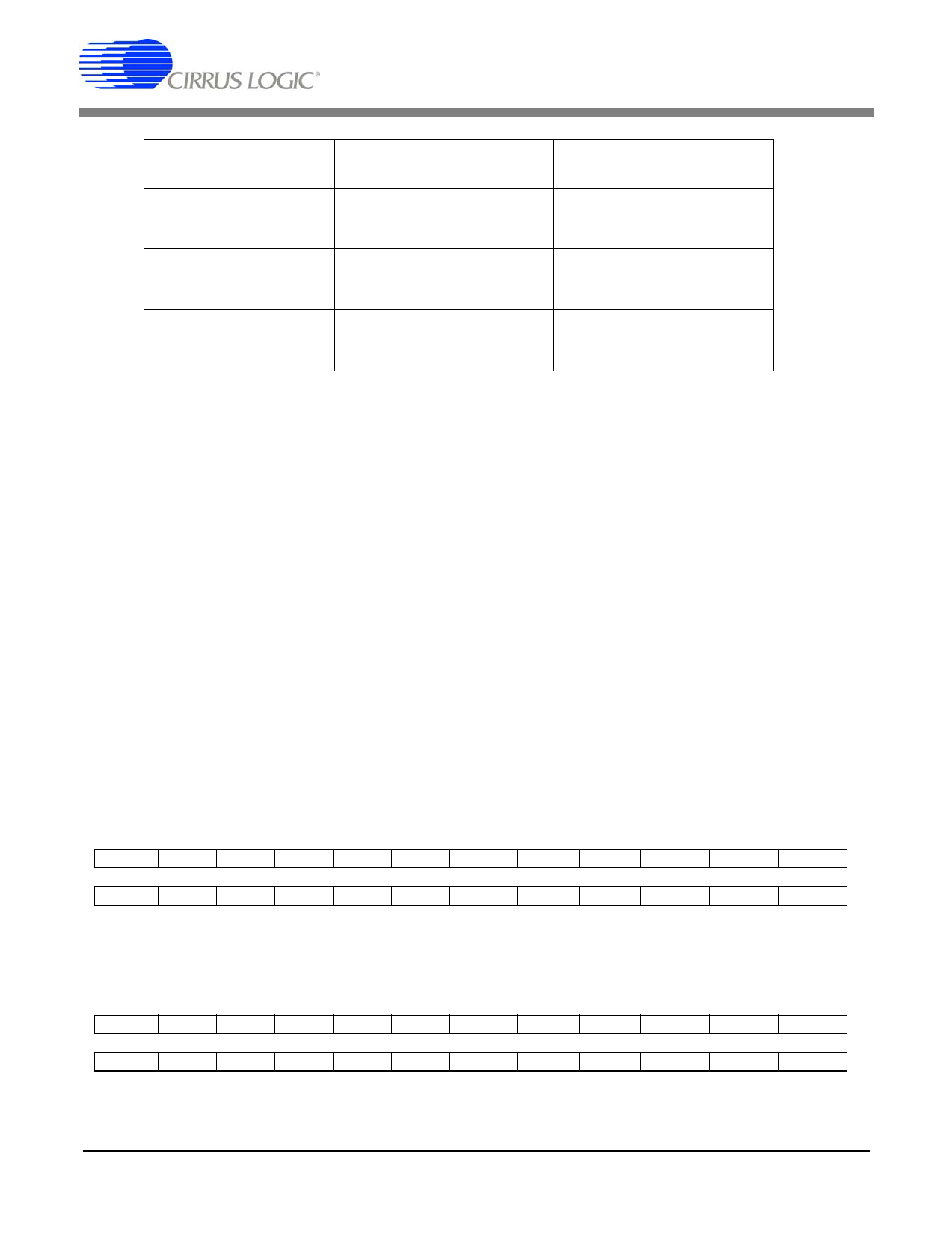
CS5511(2000) Ver la hoja de datos (PDF) - Cirrus Logic
Número de pieza
componentes Descripción
Lista de partido
CS5511 Datasheet PDF : 26 Pages
| |||
CS5510/11/12/13
2.5.3 Output Coding
As shown in Tables 1 and 2, the CS5510/11/12/13
present output conversions as 24-bit conversion
words. The first bit of the conversion word indi-
cates that a conversion is done through SDO falling
from a logic high to a logic low level. The first and
the fourth bits output will always be zero. The sec-
ond and third bits are error flags, representing an
overflow or oscillation condition. In the
CS5510/11, there are four more bits of zero, and
the remaining 16 bits are the conversion data, out-
put MSB first (Table 2). In the CS5512/13, the fi-
nal 20 bits are the conversion data, which is output
MSB first (Table 1).
Bits D22-D21 are the two flag bits. The OF (Over-
range Flag) bit is set to a logic 1 any time the input
signal is more positive than positive full scale, or
more negative than negative full scale. It is cleared
back to logic 0 whenever a conversion word occurs
which is not overranged. The OD (Oscillation De-
tect) bit is set to a logic 1 any time that an oscillatory
condition is detected in the modulator. This does
not occur under normal operating conditions, but
may occur whenever the input to the converter is ex-
cessively overranged. If the OD bit is set, the conver-
sion data bits can be completely erroneous. The OD
flag bit will be cleared to logic 0 four output words
after the modulator becomes stable again. The OD
flag can occur independent of OF with a spike on
the input. Both flag bits should be tested if any
overrange condition occurs.
Table 3 illustrates the output coding for the
CS5510/11/12/13. Conversions are output as two’s
complement values representing bipolar input sig-
nals.
2.5.4 Digital Filter
The CS5510/11/12/13 have a modified Sinc4 digi-
tal filter that provides CLK/612 Hz conversion
rates (CLK represents SCLK for the CS5510/12
and the internal oscillator for the CS5511/13). The
filters are optimized to yield better than 80 dB re-
jection between 47 Hz to 63 Hz (i.e. 80 dB mini-
mum rejection for both 50 Hz and 60 Hz) when the
master clock is 32.768 kHz. The filter has a re-
sponse as shown in Figure 20. Table 4 shows the
filter response for frequencies from 38 Hz to
71 Hz. Note that the response of the CS5511/13
will be similar, but the frequencies scale with the
on-chip oscillator’s frequency, which can be from
32 kHz to 96 kHz (i.e. conversion rates can vary
between 53 Hz to 159 Hz). Further note that after
initial power up, or after returning from sleep
mode, the filter requires four conversion cycles to
produce a valid conversion due to the modified
Sinc4 filter characteristics.
D23 D22 D21 D20 D19 D18
D17
D16 D15
D14
D13
D12
0
OF
OD
0
MSB 18
17
16
15
14
13
12
D11
D10
D9
D8
D7
D6
D5
D4
D3
D2
D1
D0
11
10
9
8
7
6
5
4
3
2
1
LSB
Table 1. CS5512/13 Output Conversion Data Register Description (Flags + 20 bits).
D23 D22 D21 D20 D19 D18
D17
D16 D15
D14
D13
D12
0
OF
OD
0
0
0
0
0
MSB
14
13
12
D11
D10
D9
D8
D7
D6
D5
D4
D3
D2
D1
D0
11
10
9
8
7
6
5
4
3
2
1
LSB
Table 2. CS5510/11 Output Conversion Data Register Description (Flags + 16 bits).
18
DS337F1
Share Link: 