CS5512-BS Ver la hoja de datos (PDF) - Cirrus Logic
Número de pieza
componentes Descripción
Lista de partido
CS5512-BS Datasheet PDF : 24 Pages
| |||
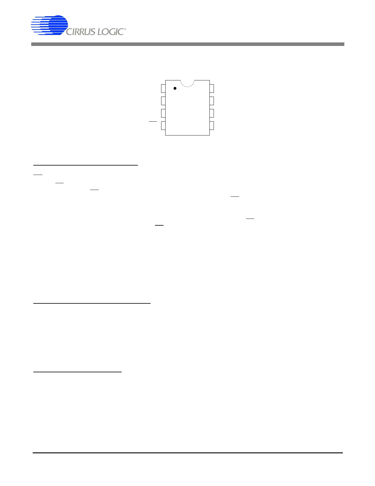
3. PIN DESCRIPTIONS
VREF 1
AIN+ 2
AIN- 3
CS 4
8 SDO
7 V-
6 V+
5 SCLK
CS5510/11/12/13
Control Pins and Serial Data I/O
CS - Chip Select, Pin 4
CS is a dual function pin, which determines the state of SDO, as well as the digital logic-low output
level. When CS is low, SDO will be active. When high, the SDO pin will output a high-impedance state.
The logic-low level of SDO will match the active-low voltage on CS.
SDO - Serial Data Output, Pin 8
SDO is the serial data output. It will output a high-impedance state if CS = 1. The logic-low level of SDO
will match the active-low voltage on CS.
SCLK - Serial Clock Input, Pin 5
SCLK is the serial bit-clock which controls the shifting of data from the ADCs. This input goes through a
Schmitt trigger to allow for slow rise and fall time signals. If held high, the device will enter sleep mode.
In the CS5510/12, this input is also used as a master clock source which determines conversion speeds
and throughput. In the CS5511/13, SCLK is only used to read the conversion data and put the part in
sleep mode.
Measurement and Reference Inputs
AIN+, AIN- - Differential Analog Input, Pins 2, 3
Differential input pins into the device
VREF - Voltage Reference Input, Pin 1
Input Voltage which establishes the voltage reference, with respect to V-, for the on-chip modulator
Power Supply Connections
V+ - Positive Power, Pin 6
Positive supply voltage
V- - Negative Supply, Pin 7
Negative supply voltage
DS337F3
21
Share Link: 