CS5531-AS Ver la hoja de datos (PDF) - Cirrus Logic
Número de pieza
componentes Descripción
Lista de partido
CS5531-AS Datasheet PDF : 50 Pages
| |||
CS5531/32/33/34-AS
instrumentation amplifier is typically 1200 pA
over -40°C to +85°C (MCLK=4.9152 MHz).
The common-mode plus signal range of the instru-
mentation amplifier is (VA-) + 0.7 V to (VA+) -
1.7 V.
Figure 4 illustrates the input models for the ampli-
fiers. The dynamic input current for each of the
pins can be determined from the models shown.
Gain = 2, 4, 8, 16, 32, 64
AIN
Vos ≤ 8 mV
in = fVos C
C = 3 .9 pF
f = MCLK
128
Gain = 1
φ1 Fine
φ1 Coarse
AIN
Vos ≤ 12 mV
in = fVos C
f = MCLK
16
C = 14 pF
Figure 4. Input models for AIN+ and AIN- pins
Note:
The C=3.9pF and C = 14pF capacitors are
for input current modeling only. For physical
input capacitance see ‘Input Capacitance’
specification under Analog Characteristics.
2.1.1. Analog Input Span
The full-scale input signal that the converter can
digitize is a function of the gain setting and the ref-
erence voltage connected between the VREF+ and
VREF- pins. The full-scale input span of the con-
verter is [(VREF+) - (VREF-)]/(GxA), where G is
the gain of the amplifier and A is 2 for VRS = 0, or
A is 1 for VRS = 1. VRS is the Voltage Reference
Select bit, and must be set according to the differen-
tial voltage applied to the VREF+ and VREF- pins
on the part. See section 2.3.5 for more details.
After reset, the unity gain buffer is engaged. With a
2.5V reference this would make the full-scale input
range default to 2.5 V. By activating the instrumen-
tation amplifier (i.e. a gain setting other than 1) and
using a gain setting of 32, the full-scale input range
can quickly be set to 2.5/32 or about 78 mV. Note
that these input ranges assume the calibration regis-
ters are set to their default values (i.e. Gain = 1.0 and
Offset = 0.0).
2.1.2. Multiplexed Settling Limitations
The settling performance of the CS5531/32/33/34
in multiplexed applications is affected by the sin-
gle-pole, low-pass filter which follows the instru-
mentation amplifier (see Figure 3). To achieve data
sheet settling and linearity specifications, it is rec-
ommended that a 22 nF C0G capacitor be used.
Capacitors as low as 10 nF or X7R type capacitors
can also be used with some minor increase in dis-
tortion for AC signals.
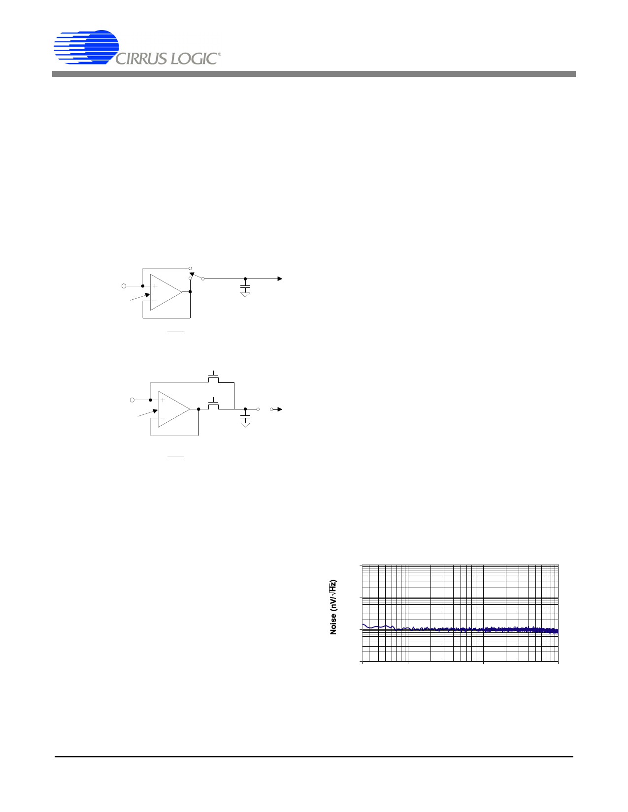
2.1.3. Voltage Noise Density Performance
Figure 5 illustrates the measured voltage noise
density versus frequency from 0.025 Hz to 10 Hz
of a CS5532-AS. The device was powered with
±2.5 V supplies, using 30 Sps OWR, the 64x gain
range, bipolar mode, and with the input short bit
enabled.
1000
100
10
1
0.025
0.10
1.00
Frequency (Hz)
10.00
Figure 5. Measured Voltage Noise Density, 64x
DS289F5
13
Share Link: 