V54C316162V Ver la hoja de datos (PDF) - Mosel Vitelic, Corp
Número de pieza
componentes Descripción
Lista de partido
V54C316162V
200/183/166/143 MHz 3.3 VOLT/ 4K REFRESH ULTRA HIGH PERFORMANCE 1M X 16 SDRAM 2 BANKS X 512Kbit X 16
Mosel Vitelic, Corp

V54C316162V Datasheet PDF : 21 Pages
| |||
MOSEL VITELIC
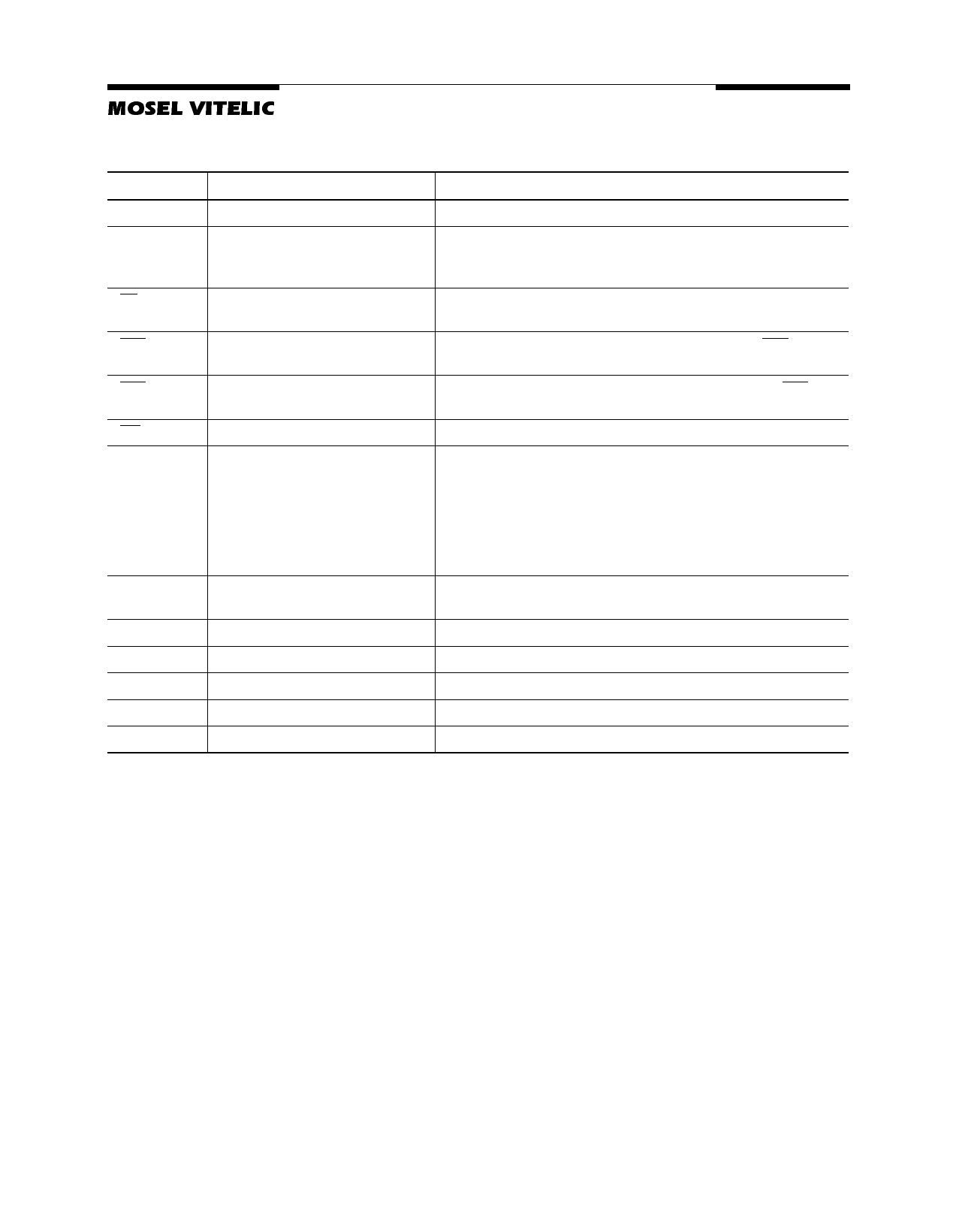
Signal Pin Description
Pin
CLK
CKE
Name
Clock Input
Clock Enable
CS
RAS
CAS
WE
A0-A10
Chip Select
Row Address Strobe
Column Address Strobe
Write Enable
Address
BA
Bank Select
I/O1-I/O16
UDQM, LDQM
Data Input/Output
Data Input/Output Mask
VDD/VSS
Power Supply/Ground
VDDQ/VSSQ Data Output Power/Ground
NC
No Connection
V54C316162V
Input Function
System clock input. Active on the positive rising edge to sample all inptus
Activates the CLK signal when high and deactivates the CLK when low.
CKE low initiates the power down mode, suspend mode, or the self
refresh mode
Disables or enables device operation by masking or enabling all inputs
except CLK, CKE and DQMi
Latches row addresses on the positive edge of CLK with RAS low.
Enables row access & precharge
Latches column addresses on the positive edge of CLK with CAS low.
Enables column access
Enables write operation
During a bank activate command, A0-A10 defines the row address.
During a read or write command, A0-A7 defines the column address. In
addition to the column address A10 is used to invoke auto precharge BA
define the bank to be precharged. A10 is low, auto precharge is disabled
during a precharge cycle, If A10 is high, both bank will be precharged ,
if A10 is low, the BA is used to decide which bank to precharge. If A10 is
high, all banks will be precharged.
Selects which bank to activate. BA low select bank A and high selects
bank B
Data inputs/output are multiplexed on the same pins
Makes data output Hi-Z. Blocks data input when DQM is active
Power Supply. +3.3V ± 0.3V/ground
Provides isolated power/ground to DQs for improved noise immunity
V54C316162V Rev.2.9 September 2001
4
Share Link: