MAX8631X(2006) Ver la hoja de datos (PDF) - Maxim Integrated
Número de pieza
componentes Descripción
Lista de partido
MAX8631X
(Rev.:2006)
(Rev.:2006)
Maxim Integrated

MAX8631X Datasheet PDF : 16 Pages
| |||
1x/1.5x/2x White LED Charge Pump with Two
LDOs in 4mm x 4mm Thin QFN
1µF
1µF
INPUT
2.7V TO 5.5V
10µF
C1P C1N
PIN
IN
GND
C2P C2N
LDO1
LDO2
ON/OFF AND
VOLTAGE
SELECTION
OUT
MAX8631X
ENM2
MAX8631Y
ENM1
ENF
ENLDO
P1
P2
SETM SETF REFBP
M1
M2
M3
M4
F1
F2
F3
F4
PGND
6.81kΩ 4.12kΩ
0.01µF
1µF
1µF
OUTPUT
UP TO 240mA
10µF MAIN
FLASH
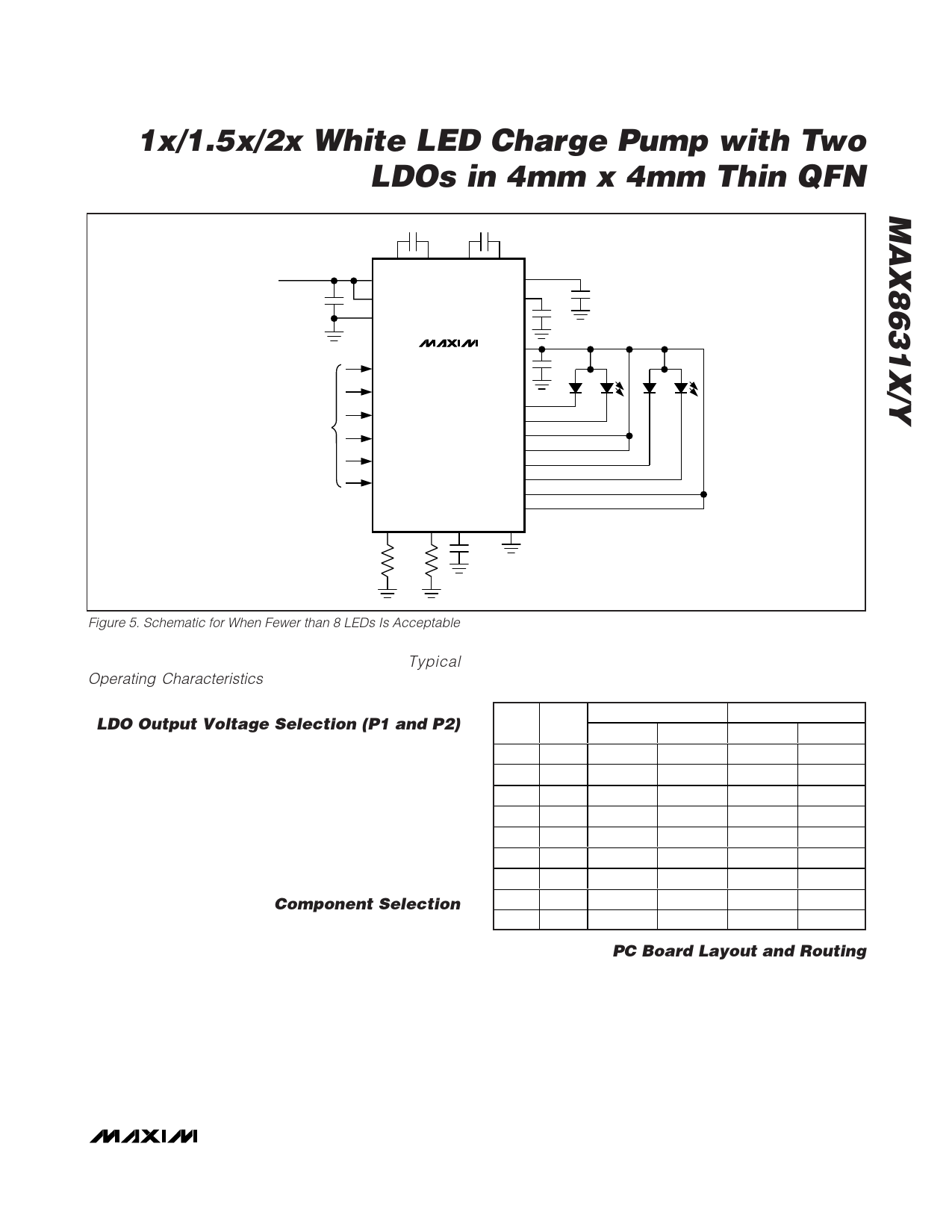
Figure 5. Schematic for When Fewer than 8 LEDs Is Acceptable
Input Ripple
For LED drivers, input ripple is more important than out-
put ripple. Input ripple is highly dependent on the
source supply’s impedance. Adding a lowpass filter to
the input further reduces input ripple. Alternately,
increasing CIN to 22µF cuts input ripple in half with only
a small increase in footprint. The 1x mode always has
very low input ripple.
Typical operating waveforms shown in the Typical
Operating Characteristics show input ripple current in
1x, 1.5x, and 2x mode.
LDO Output Voltage Selection (P1 and P2)
As shown in Table 2, the LDO output voltages, LDO1
and LDO2 are pin-programmable by the logic states of
P1 and P2. P1 and P2 are tri-level inputs: IN, open, and
GND. The input voltage, VIN, must be greater than the
selected LDO1 and LDO2 voltages. The logic states of
P1 and P2 can be programmed only during ENLDO
low. Once the LDO_ voltages are programmed, their
values do not change by changing P1 or P2 during
ENLDO high.
Component Selection
Use only ceramic capacitors with an X5R, X7R, or better
dielectric. See Table 3 for a list of recommended parts.
Table 2. P1 and P2, LDO Output Voltage
Selection
P1
IN
IN
IN
OPEN
OPEN
OPEN
GND
GND
GND
P2
IN
OPEN
GND
IN
OPEN
GND
IN
OPEN
GND
MAX8631X
MAX8631Y
LDO1 (V) LDO2 (V) LDO1 (V) LDO2 (V)
3.3
1.8
2.8
2.6
3.0
1.5
2.8
2.8
2.8
1.5
2.9
1.5
3.3
1.5
2.6
1.9
2.6
1.8
2.6
2.6
2.6
1.5
2.8
1.9
3.0
1.8
2.9
1.8
2.8
1.8
2.9
1.9
2.5
1.8
2.9
2.9
Connect a 1µF ceramic capacitor between LDO1 and
GND, and a second 1µF ceramic capacitor between
LDO2 and GND for 200mA applications. The LDO out-
put capacitor’s (CLDO) equivalent series resistance
(ESR) affects stability and output noise. Use output
capacitors with an ESR of 0.1Ω or less to ensure stability
and optimum transient response. Connect CLDO_ as
close to the MAX8631X/Y as possible to minimize the
impact of PC board trace inductance.
______________________________________________________________________________________ 13
Share Link: