5P49V5901BDDDNLGI Ver la hoja de datos (PDF) - Integrated Device Technology
Número de pieza
componentes Descripción
Lista de partido
5P49V5901BDDDNLGI Datasheet PDF : 37 Pages
| |||
5P49V5901 DATASHEET
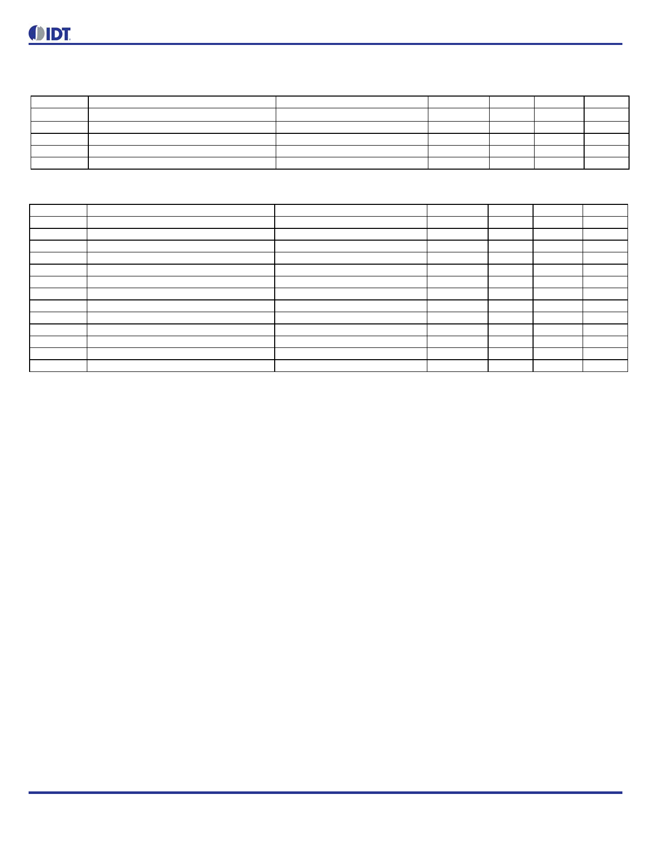
Table 6: I2C Bus DC Characteristics
Symbol
VIH
VIL
VHYS
IIN
VOL
Parameter
Input HIGH Level
Input LOW Level
Hysteresis of Inputs
Input Leakage Current
Output LOW Voltage
Conditions
Min
For SEL1/SDA pin and SEL0/SCL pin 0.7xVDDD
For SEL1/SDA pin and SEL0/SCL pin GND-0.3
0.05xVDDD
-1
IOL = 3 mA
Typ
Max
Unit
5.5 2
V
0.3xVDDD V
V
30
µA
0.4
V
Table 7: I2C Bus AC Characteristics
Symbol
Parameter
FSCLK Serial Clock Frequency (SCL)
tBUF Bus free time between STOP and START
tSU:START Setup Time, START
tHD:START Hold Time, START
tSU:DATA Setup Time, data input (SDA)
tHD:DATA Hold Time, data input (SDA) 1
tOVD Output data valid from clock
CB
Capacitive Load for Each Bus Line
tR
Rise Time, data and clock (SDA, SCL)
tF
Fall Time, data and clock (SDA, SCL)
tHIGH HIGH Time, clock (SCL)
tLOW LOW Time, clock (SCL)
tSU:STOP Setup Time, STOP
Min
Typ
Max
Unit
10
400
kHz
1.3
µs
0.6
µs
0.6
µs
0.1
µs
0
µs
0.9
µs
400
pF
20 + 0.1xCB
300
ns
20 + 0.1xCB
300
ns
0.6
µs
1.3
µs
0.6
µs
Note 1: A device must internally provide a hold time of at least 300 ns for the SDA signal (referred to the VIH(MIN) of the SCL signal) to bridge the
undefined region of the falling edge of SCL.
Note 2: I2C inputs are 5V tolerant.
MARCH 3, 2017
11
PROGRAMMABLE CLOCK GENERATOR
Share Link: 