PI3VT3306UX Ver la hoja de datos (PDF) - Pericom Semiconductor
Número de pieza
componentes Descripción
Lista de partido
PI3VT3306UX Datasheet PDF : 5 Pages
| |||
PI3VT3306
2-Bit, 2-Port, Low Voltage
Translator Bus Switch
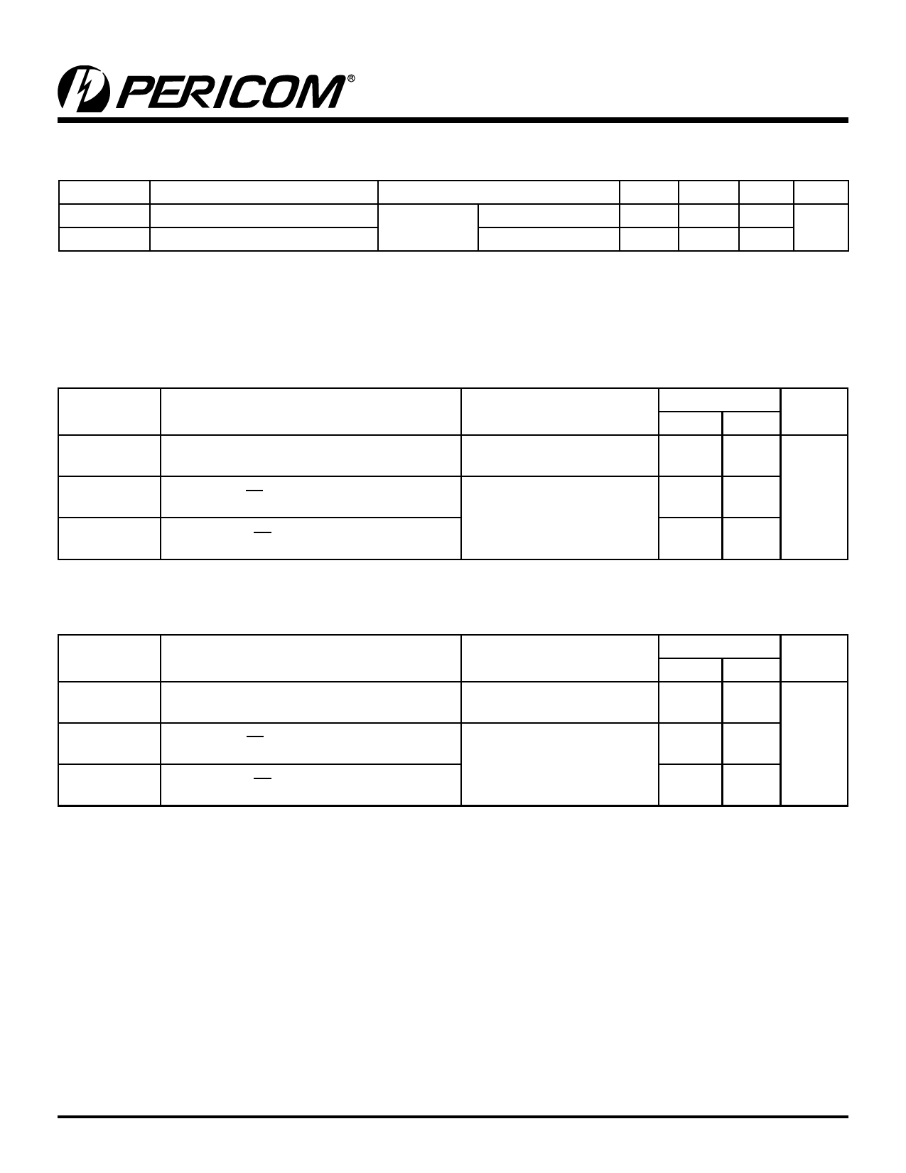
Power Supply Characteristics
Parameters
Description
Test Conditions(1)
Min. Typ.(2) Max.
ICC
∆ICC
Quiescent Power Supply Current
Quiescent Current per Input HIGH
VCC = Max.
VIN = GND or VCC
VIN = 3V(3)
3
50
Notes:
1. For Max. or Min. conditions, use appropriate value specified under Electrical Characteristics for the applicable device.
2. Typical values are at VCC = 3.3V, +25°C ambient.
3. Per driven input (control input only); A and B pins do not contribute to ∆ICC.
Units
µA
Switching Characteristics over 3.3V ±0.3V Operating Range
Parameters
Description
Conditions(1)
tPLH
tPHL
Propogation Delay(2,3) Ax to Bx
tPZH
tPZL
Enable Time BE to Ax or Bx
tPHZ
tPLZ
Disable Time BE to Ax or Bx
CL = 50pF,
RL = 500Ω
CL = 50pF,
RL = 500Ω,
R = 500Ω
Com.
Min. Max.
0.25
Units
1.5
6.5
ns
1.5
5.5
Switching Characteristics over 2.5V ±0.2V Operating Range
Parameters
Description
Conditions(1)
Com.
Min. Max.
Units
tPLH
tPHL
Propogation Delay(2,3) Ax to Bx
CL = 50pF,
RL = 500Ω
0.25
tPZH
tPZL
Enable Time BE to Ax or Bx
tPHZ
tPLZ
Disable Time BE to Ax or Bx
CL = 50pF,
RL = 500Ω,
R = 500Ω
1.5
9.8
ns
1.5
8.3
Notes:
1. See test circuit and waveforms.
2. This parameter is guaranteed but not tested on Propagation Delays.
3. The bus switch contributes no propagational delay other than the RC delay of the On-Resistance of the switch and the load
capacitance. The time constant for the switch alone is of the order of 0.25ns for 50pF load. Since this time constant is much
smaller than the rise/fall times of typical driving signals, it adds very little propagational delay to the system. Propagational de-
lay of the bus switch when used in a system is determined by the driving circuit on the driving side of the switch and its interac-
tion with the load on the driven side.
3
PS8533B
11/10/04
Share Link: 