RF2472G Ver la hoja de datos (PDF) - RF Micro Devices
Número de pieza
componentes Descripción
Lista de partido
RF2472G Datasheet PDF : 12 Pages
| |||
RF2472
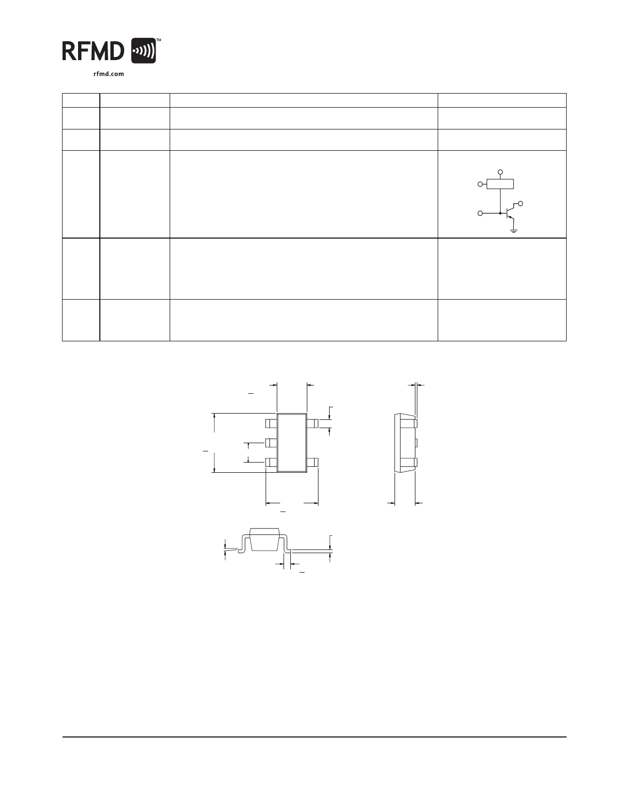
Pin Function Description
Interface Schematic
1
VCC
Supply connection. An external bypass capacitor may be required in some See pin 3.
applications.
2
GND
Ground connection. Keep traces physically short and connect immediately
to ground plane for best performance.
3
RF IN
RF input pin. This pin is DC coupled and matched to 50Ω at 2.4GHz.
VCC
PD
BIAS
RF IN
RF OUT
4
PD
Power down pin.This pin enables the bias to the amplifier. To turn the
amplifier on, this pin should be connected to VCC. Connecting this pin to
ground, will turn the amplifier off and reduce the current draw to below
1μA. This pin is a CMOS input. There is no DC current draw other than the
transient current required to charge or discharge the gate capacitance
(less than 5pF).
5
RF OUT
LNA Output pin.This pin is an open-collector output. It must be biased to See pin 3.
VCC through a choke or matching inductor. This pin is typically matched to
50Ω with a shunt bias/matching inductor and series blocking/matching
capacitor. Refer to application schematics.
Package Drawing
1.60
0.15
+ 0.01
0.05
0.400
1
2.90
+ 0.10 0.950
3° MAX
0° MIN
2.80
+ 0.20
0.127
1.44
1.04
Dimensions in mm.
0.45
+ 0.10
Rev A11 DS080128
7628 Thorndike Road, Greensboro, NC 27409-9421 · For sales or technical
support, contact RFMD at (+1) 336-678-5570 or sales-support@rfmd.com.
3 of 12
Share Link: 