JANTX2N6804 Ver la hoja de datos (PDF) - Microsemi Corporation
Número de pieza
componentes Descripción
Lista de partido
JANTX2N6804 Datasheet PDF : 7 Pages
| |||
2N6804
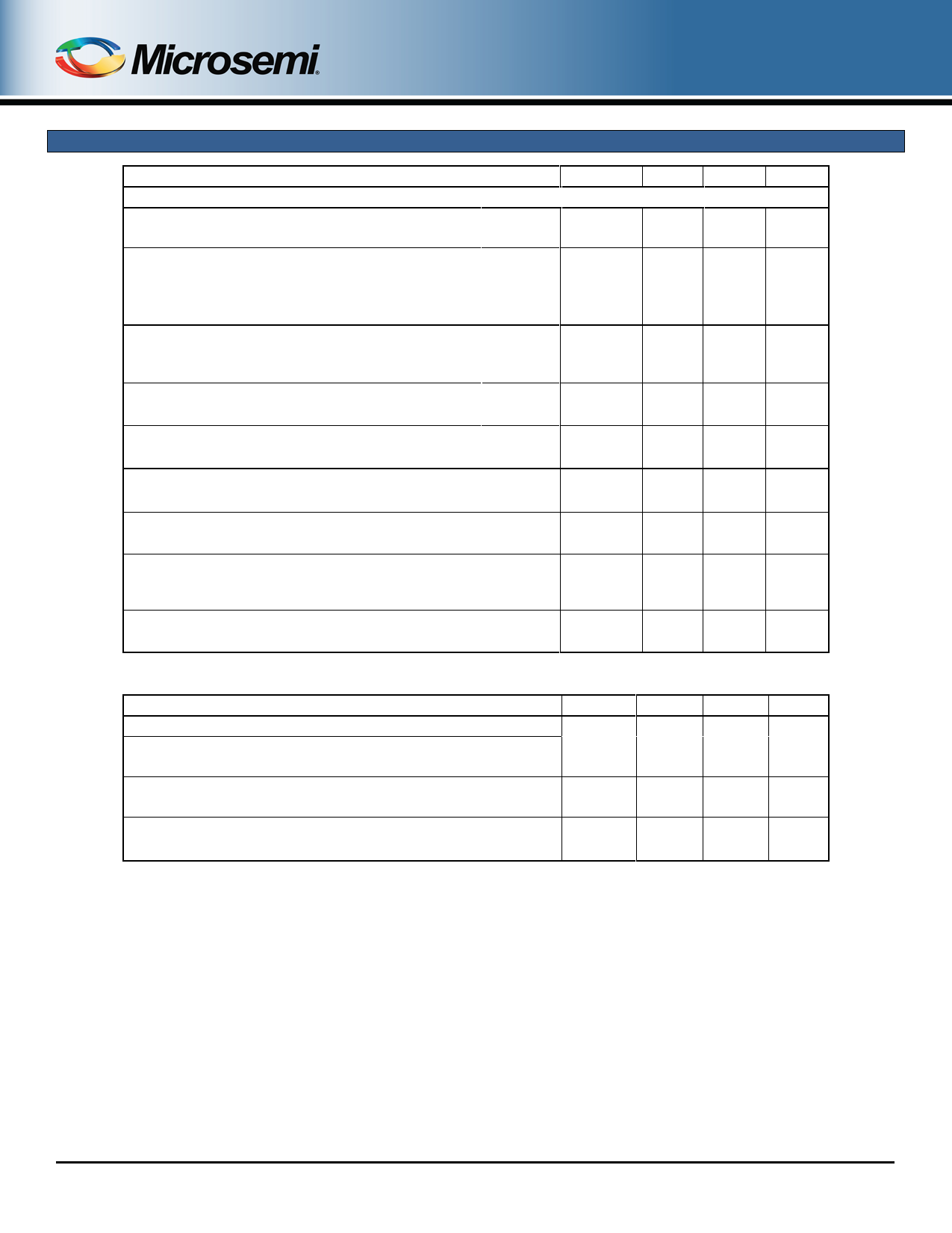
ELECTRICAL CHARACTERISTICS @ TA = +25 °C, unless otherwise noted
Parameters / Test Conditions
OFF CHARACTERISTICS
Drain-Source Breakdown Voltage
VGS = 0 V, ID = -1.0 mA
Gate-Source Voltage (Threshold)
VDS ≥ VGS, ID = -0.25 mA
VDS ≥ VGS, ID = -0.25 mA, TJ = +125 °C
VDS ≥ VGS, ID = -0.25 mA, TJ = -55 °C
Gate Current
VGS = ± 20 V, VDS = 0 V
VGS = ± 20 V, VDS = 0 V, TJ = +125 °C
Drain Current
VGS = 0 V, VDS = -80 V
Drain Current
VGS = 0 V, VDS = -80 V, TJ = +125 °C
Static Drain-Source On-State Resistance
VGS = -10 V, ID = -7 A pulsed
Static Drain-Source On-State Resistance
VGS = -10 V, ID = -11 A pulsed
Static Drain-Source On-State Resistance
TJ = +125°C
VGS = -10 V, ID = -7 A pulsed
Diode Forward Voltage
VGS = 0 V, IS = -11.0 A pulsed
Symbol Min. Max.
V(BR)DSS -100
V GS(th)1
V GS(th)2
V GS(th)3
I GSS1
I GSS2
I DSS1
I DSS2
r DS(on)1
r DS(on)2
-2.0 -4.0
-1.0
-5.0
±100
±200
-25
0.25
0.30
0.36
r DS(on)3
V SD
0.55
-4.7
Unit
V
V
nA
µA
mA
Ω
Ω
Ω
V
DYNAMIC CHARACTERISTICS
Parameters / Test Conditions
Gate Charge:
On-State Gate Charge
VGS = -10 V, ID = -11 A, VDS = -50 V
Gate to Source Charge
VGS = -10 V, ID = -11 A, VDS = -50 V
Gate to Drain Charge
VGS = -10 V, ID = -11 A, VDS = -50 V
Symbol Min. Max. Unit
Q g(on)
Q gs
Q gd
29.0 nC
7.1
nC
21.0 nC
T4-LDS-0113, Rev. 3 (121514)
©2012 Microsemi Corporation
Page 3 of 7
Share Link: 