PI3C6800 Ver la hoja de datos (PDF) - Pericom Semiconductor
Número de pieza
componentes Descripción
Lista de partido
PI3C6800
Pericom Semiconductor

PI3C6800 Datasheet PDF : 5 Pages
| |||
PI3C6800
2.5V/3.3V, 2-Port, 10-Bit Bus Switch with
112233445566778899001122334455667788990011223344556677889900112211223344556677889900112233445566778899001122334455667788990011221122334455667788990011223344556677889900112233445566P7788r9900e11c22h1122a3344r55g66e7788d9900O1122u3344t55p6677u8899t00s11f22o3344r5566L7788i99v00e1122I11n2233s44e55r6677t88i99o00n1122
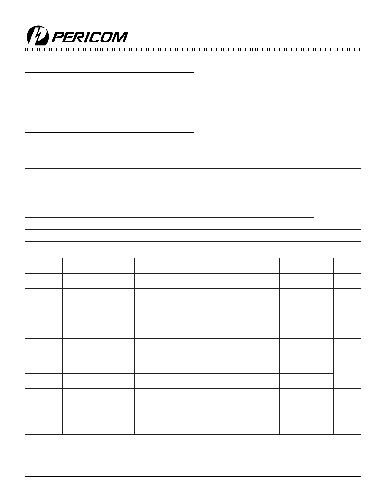
Absolute Maximum Ratings Over Free-Air Temperature Range*
(Above which the useful life may be impaired. For user guidelines, not tested.)
1
Storage Temperature ........................................ 65°Cto+150°C
Supply Voltage Range .......................................... 0.5Vto4.6V
DC Input Voltage(1) ............................................... 0.5Vto+7V
Input Clamp Current, IIK (V1< 0) .....................................50mA
DC Output Current ......................................................... 120mA
Power Dissipation(2) .......................................................... 0.5W
Note:
2 Stresses greater than those listed under MAXIMUM RATINGS
may cause permanent damage to the device. This is a stress rating
only and functional operation of the device at these or any other
conditions above those indicated in the operational sections of
3 this specification is not implied. Exposure to absolute maximum
rating conditions for extended periods may affect reliability.
Notes:
1. Input and output negative-voltage ratings may be exceeded if the input and output clamp-current ratings are observed.
2. Maximum package power dissipation is calculated using a junction temperatue of 150°C and a board trace length of 750 mils.
4
Recommended Operating Conditions
VCC
Supply voltage
Min.
Typ.
Units
5
2.3
3.3
BIASV
VIH
VIL
Supply voltage
High-level input voltage
Low-level input voltage
1.3
VCC
V
2
6
0.8
TA
Operating free-air temperature
40
85
Electrical Characteristics (Over Recommended Operating Free-air Temperature Range)
°C
7
Parameters
Description
VIK
Clamp Diode Voltage
II
Input Current
Test Conditions
VCC = 3.0V, IIN = 18mA
VCC = 3.6V, VIN = VCC or GND
Min. Typ.
Max.
1.2
±5
8 Units
V
µA 9
IO
Output Current
VCC = 3.0V, BIASV = 2.4V, VO = 0
0.25
ICC
Quiescent Power Supply
Current
VCC = 3.6V, IO = 0, VIN = VCC or GND
260
500
∆ICC
Power Supply Current per VCC = 3.6V, One input at 2.7V
Input
Other at VCC or GND
2.5
CIN
Input Capacitance
VCC = 0V
3.5
COFF A/B Capacitance
VCC = 0V, Switch Off
5.0
RON*
Switch ONResistance
VIN = 0, IIN = 64mA
VCC = 3.0V VIN = 2.4V, IIN = 30mA
5
7
8.0
15
mA 10
µA
11
mA
12
pF
13
14
Ω
VIN = 2.4V, IIN = 15mA
8.0
15
Notes:
* Measured by the voltage drop between the A and B terminals at the indicated current through the switch.
On-state resistance is determined by the lower of the voltages of the two (A or B) terminals.
This is the increase in supply current for control input.
All typical values are at VCC = 3.3V, TA = 25°C.
15
2
PS8191D 05/03/00
Share Link: