PI2BV3877 Ver la hoja de datos (PDF) - Pericom Semiconductor
Número de pieza
componentes Descripción
Lista de partido
PI2BV3877 Datasheet PDF : 4 Pages
| |||
PI2BV3877
2.5V, 10-Bit, 2-Port
266 MHz DDR Bus Switch 1122334455667788990011223344556677889900112233445566778899001122112233445566778899001122334455667788990011223344556677889900112211223344556677889900112233445566778899001122334455667788990011221122334455667788990011223344556677889900112233445566778899001122112233445566778899001122
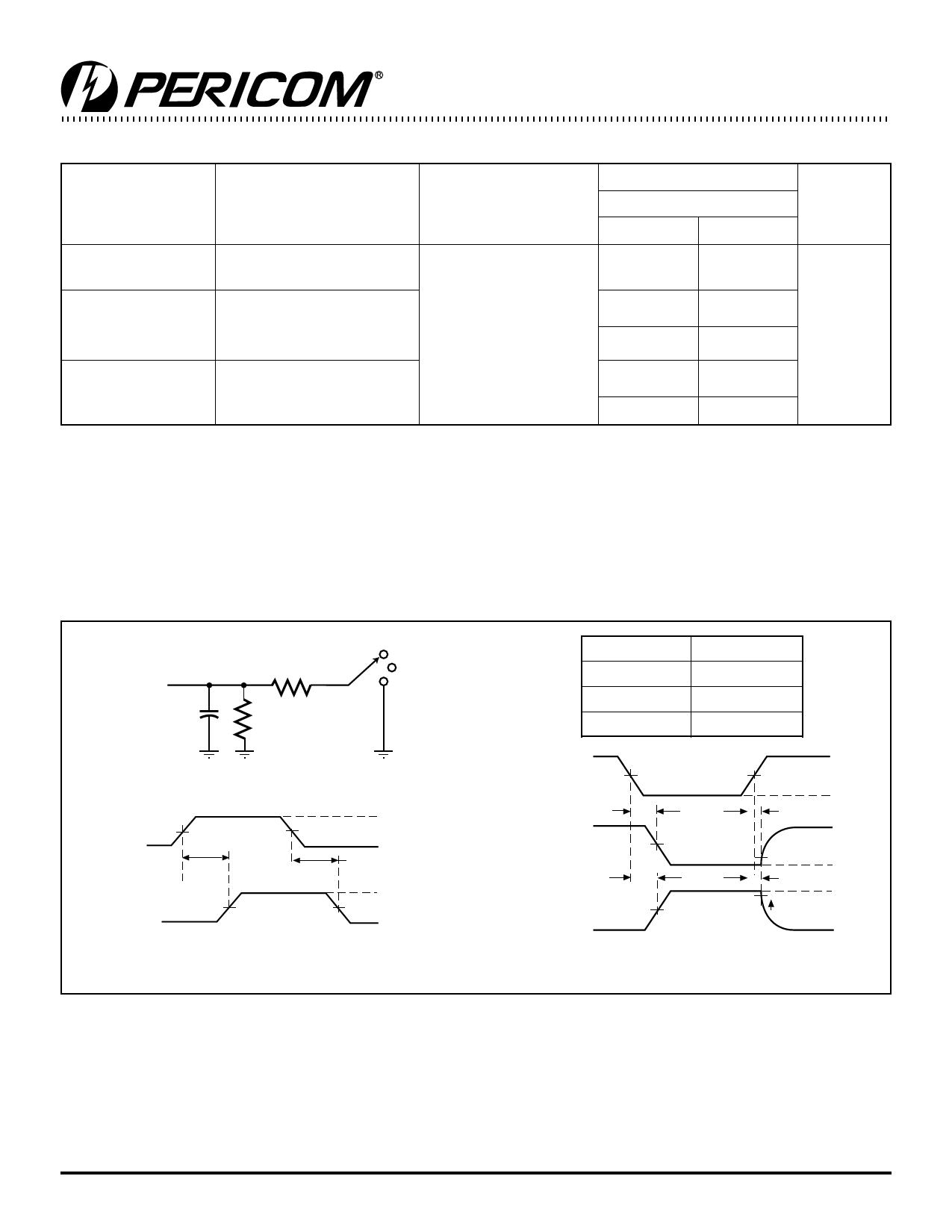
Switching Characteristics over Operating Range
Parameters
tPLH
tPHL
Description
Propagation Delay(2,3)
Ax to Bx, Bx to Ax
Conditions(2,3)
PI2BV3877
Com.
Min.
Max.
1
Units
tPZH
Bus Enable Time
tPZL
BE to Ax or Bx
tPHZ
Bus Disable Time
tPLZ
BE to Ax or Bx
CL = 30pF,
RL = 500 ohms,
R = 500 ohms
1
3
1
3.5
ns
1
3
1
3.8
Notes:
1. See test circuit and waveforms.
2. This parameter is guaranteed but not tested on Propagation Delays.
3. The bus switch contributes no propagational delay other than the RC delay of the ON resistance of the switch and the load capacitance.
The time constant for the switch alone is of the order of 1ns for 50pF load. Since this time constant is much smaller than the rise/
fall times of typical driving signals, it adds very little propagational delay to the system. Propagational delay of the bus switch when
used in a system is determined by the driving circuit on the switch's driving side and its interaction with the load on the driven side.
Parameter Measurements
From Output
Under Test
CL = 30pF
(See note 1)
500Ω
500Ω
2xVCC
S1
Open
GND
LOAD CIRCUIT
Input
tPLH
VCC/2
VCC/2
tPHL
VCC
0V
Output
VCC/2
VOH
VCC/2
VOL
VOLTAGE WAVEFORMS
PROPAGATION DELAY TIMES
Test
tPD
tPLZ/tPZL
tPHZ/tPZH
S1
Open
2xVCC
GND
Output
Control
(Low Level
Enabling)
Output
Waveform 1
S1 at 2xVCC
(see Note 2)
Output
Waveform 2
S1 at GND
(see Note 2)
tPZL
tPZH
VCC/2
VCC/2
VCC/2
VCC/2
tPLZ
VCC
0V
VOH
VOL +0.15V VOL
tPHZ
VOH
VOH -0.15V
0V
VOLTAGE WAVEFORMS
ENABLE AND DISABLE TIMES
Notes:
1. CL includes probe and jig capacitance.
2. Waveform 1 is for an output with internal conditions such that the output is LOW except when disabled by the output control.
Waveform 2 is for an output with internal conditions such that the output is HIGH except when disabled by the output control.
3. All input pulses are supplied by generators having the following characteristics: PRR<10MHz, ZO = 50 ohms, tR ≤2ns, tF ≤2ns.
4. The outputs are measured one at a time with one transition per measurement.
5. tPLZ and tPHZ are the same as tDIS.
6. tPZL and tPZH are the same as tEN.
7. tPLH and tPHL are the same as tPD.
3
PS8472D 11/14/01
Share Link: 