MB40C938V Ver la hoja de datos (PDF) - Fujitsu
Número de pieza
componentes Descripción
Lista de partido
MB40C938V Datasheet PDF : 13 Pages
| |||
MB40C938V
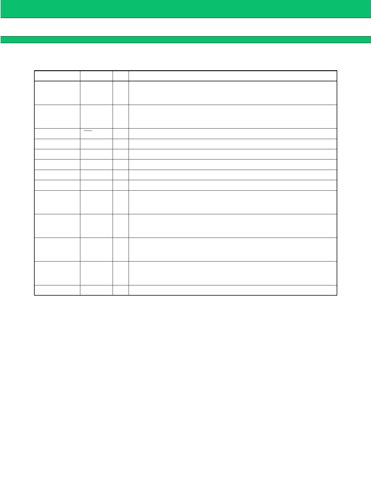
s PIN DESCRIPTION
Pin No.
4 to 11
12 to 19
20 to 27
28
29
30
47
48
40, 46
31
42, 44
36
1
37
35
2
39
34
3
38
33
45
43
41
32
Symbol
R0 to R7
G0 to G7
B0 to B7
RCLK
GCLK
BCLK
CE
DVDD
AVDD
DVSS
AVSS
VROUT
RVRIN
GVRIN
BVRIN
RIREF
GIREF
BIREF
RVB
GVB
BVB
ROUT
GOUT
BOUT
N.C.
I/O
Description
I Data signal incoming terminal for Rch, Gch and Bch
LSB: R0, G0, B0 MSB: R7, G7,B7
I Clock signal incoming terminal for Rch, Gch and Bch (3 V CMOS)
I Power saving signal incoming terminal. Power saving enabled for High
— Digital power supply terminal (standard 3 V)
— Analog power supply terminal (standard 3 V)
— Digital ground terminal
— Analog ground terminal
O Rererence voltage output terminal (standard: 1.2 V )
I Reference voltage incoming terminal for Rch, Gch and Bch
(standard: 1.2 V )
— Reference resistor connection terminal for Rch, Gch and Bch
— Connect >0.1 µF capacitor to the AVDD terminal
O Analog signal output terminals for Rch, Gch and Bch
— Not connected. To be left open.
3
Share Link: 