CBT6820 Ver la hoja de datos (PDF) - Philips Electronics
Número de pieza
componentes Descripción
Lista de partido
CBT6820
Philips Electronics

CBT6820 Datasheet PDF : 8 Pages
| |||
Philips Semiconductors
20-bit bus switch with precharged outputs and
Schottky undershoot protection for live insertion
Product specification
CBT6820
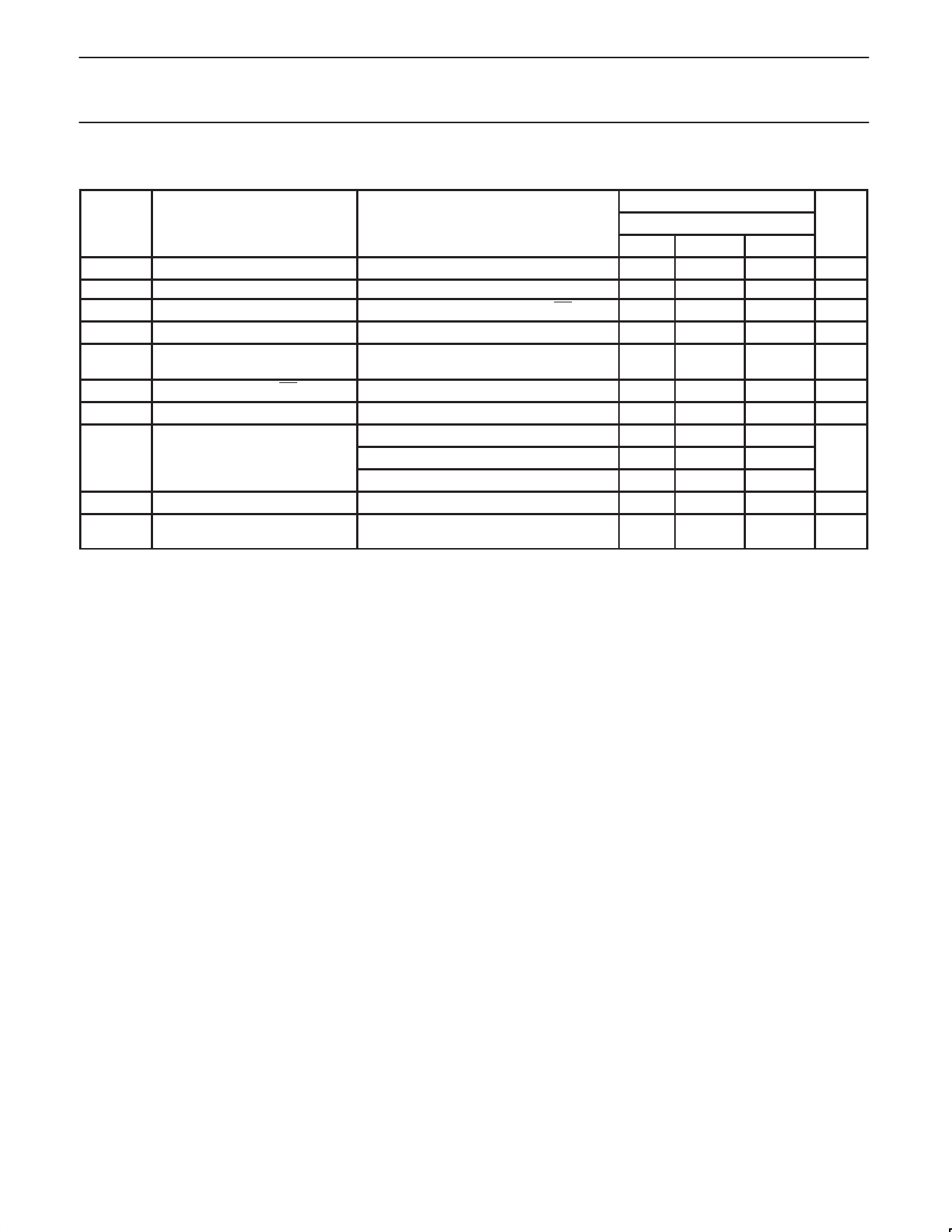
DC ELECTRICAL CHARACTERISTICS
LIMITS
SYMBOL
PARAMETER
TEST CONDITIONS
Tamb = –40°C to +85°C
Min
Typ1
Max
UNIT
VIK
Input clamp voltage
VCC = 4.5V; II = –18mA
–1.2
V
II
Input leakage current (control pin) VCC = 5.5V; VI = GND or 5.5V
IO
Output bias current (B pins)
VCC = 4.5V; BiasV = 2.4V; VO = 0, OE = VCC
±5
µA
–0.25
mA
ICC
Quiescent supply current
VCC = 5.5V; IO = 0, VI = VCC or GND
2.5
mA
∆ICC
Control pins2
VCC = 5.5V, one input at 3.4V,
other inputs at VCC or GND
2.5
mA
CI
Input capacitance per OE pin
VI= 3V or 0
4.5
pF
CO(OFF) Capacitance per port (OFF-state) VO = 3V or 0; switch off
9.5
pF
VCC = 4.5V; VI = 0V; II = 64mA
5
7
ron3
On-resistance
VCC = 4.5V; VI = 0V; II = 30mA
5
7
Ω
VCC = 4.5V; VI = 2.4V; II = –15mA
10
15
VP
Pass voltage
VIN = VCC = 4.5V; Iout = –100µA
3.4
3.6
3.9
V
IUSP
Undershoot static current
protection4
VCC = 5.0V, VBias = VCC
IB = –5µA, VB ≥ 3.0V
–10
mA
NOTES:
1. All typical values are at VCC = 5V, TA = 25 C
2. This is the increase in supply current for each input that is at the specified TTL voltage level rather than VCC or GND
3. Measured by the voltage drop between the A and the B terminals at the indicated current through the switch. On–state resistance is
determined by the lowest voltage of the two (A or B) terminals.
4. Force IUSP, measure VB ≥ 3V
1999 Apr 05
4
Share Link: