PI74ALVCH16841 Ver la hoja de datos (PDF) - Pericom Semiconductor
Número de pieza
componentes Descripción
Lista de partido
PI74ALVCH16841 Datasheet PDF : 5 Pages
| |||
PI74ALVCH16841
1122334455667788990011223344556677889900112233445566778899001122112233445566778899001122334455667788990011223344556677889900112211223344556677889900112233445566778899001122334455667788990011221122334455667788990011223344556677889900112233445566778899001122112233445566778899001122
20-Bit Bus-Interface D-Type Latch
with 3-STATE Outputs
Product Features
• PI74ALVCH16841 is designed for low voltage operation
• VCC = 2.3V to 3.6V
• Hysteresis on all inputs
• Typical VOLP (Output Ground Bounce)
< 0.8V at VCC = 3.3V, TA = 25°C
• Typical VOHV (Output VOH Undershoot)
< 2.0V at VCC = 3.3V, TA = 25°C
• Bus Hold retains last active bus state during 3-STATE,
eliminating the need for external pullup resistors
• Industrial operation at 40°C to +85°C
• Packages available:
56-pin 240 mil wide plastic TSSOP (A)
56-pin 300 mil wide plastic SSOP (V)
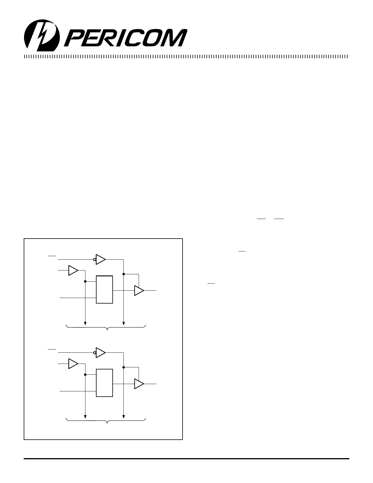
Logic Block Diagram
1
1OE
1LE 56
C1
1D1 55
1D
2 1Q1
Product Description
Pericom Semiconductors PI74ALVCH series of logic circuits are
produced in the Companys advanced 0.5 micron CMOS technology,
achieving industry leading speed.
The PI74ALVCH16841, a 20-bit bus-interface D-type latch designed
for 2.3V to 3.6V VCC operation.
The PI74ALVCH16841 features 3-state outputs designed specifically
for driving highly capacitive or relatively low-impedance loads.
It is particularly suitable for implementing buffer registers,
unidirectional bus drivers, and working registers.
The PI74ALVCH16841 can be used as two 10-bit latches or one
20-bit latch (transparent D-type). The device has non-inverting
Data (D) inputs and provides true data at its outputs. While the
Latch Enable (1LE or 2LE) input is HIGH, the Q outputs of the
corresponding 10-bit latch follow the D inputs. When LE is taken
LOW, the Q outputs are latched at the levels set up at the D inputs.
A buffered Output Enable (1OE or 2OE) input can be used to place
the outputs of the corresponding 10-bit latch in either a normal logic
state (high or low logic levels) or a high-impedance state. In that
state, outputs neither load nor drive the bus lines significantly.
The Output Enable (OE) input does not affect the internal operation
of the latches. Old data can be retained or new data can be entered
while the outputs are in the high-impedance state.
To ensure the high-impedance state during power up or power
down, OE should be tied to VCC through a pullup resistor; the
minimum value of the resistor is determined by the current-sinking
capability of the driver.
Active bus-hold circuitry is provided to hold unused or floating
data inputs at a valid logic level.
TO NINE OTHER CHANNELS
28
2OE
2LE 29
C1
2D1 42
1D
15 2Q1
TO NINE OTHER CHANNELS
1
PS8182A 11/06/00
Share Link: 