PI5C16210(2002) Ver la hoja de datos (PDF) - Pericom Semiconductor
Número de pieza
componentes Descripción
Lista de partido
PI5C16210 Datasheet PDF : 6 Pages
| |||
PI5C16210
20-Bit, 2-Port Bus Switch 1122334455667788990011223344556677889900112233445566778899001122112233445566778899001122334455667788990011223344556677889900112211223344556677889900112233445566778899001122334455667788990011221122334455667788990011223344556677889900112233445566778899001122112233445566778899001122
Maximum Ratings
(Above which the useful life may be impaired. For user guidelines, not tested.)
Storage Temperature .................................................................. –65°C to +150°C
Ambient Temperature with Power Applied ................................. –40°C to +85°C
Supply Voltage to Ground Potential (Inputs & Vcc Only) ........... –0.5V to +7.0V
Supply Voltage to Ground Potential (Outputs & D/O Only) ....... –0.5V to +7.0V
DC Input Voltage ......................................................................... –0.5V to +7.0V
DC Output Current ................................................................................... 120 mA
Power Dissipation ......................................................................................... 0.5W
Note:
Stresses greater than those listed under MAXI-
MUM RATINGS may cause permanent damage
to the device. This is a stress rating only and
functional operation of the device at these or any
other conditions above those indicated in the
operational sections of this specification is not
implied. Exposure to absolute maximum rating
conditions for extended periods may affect reli-
ability.
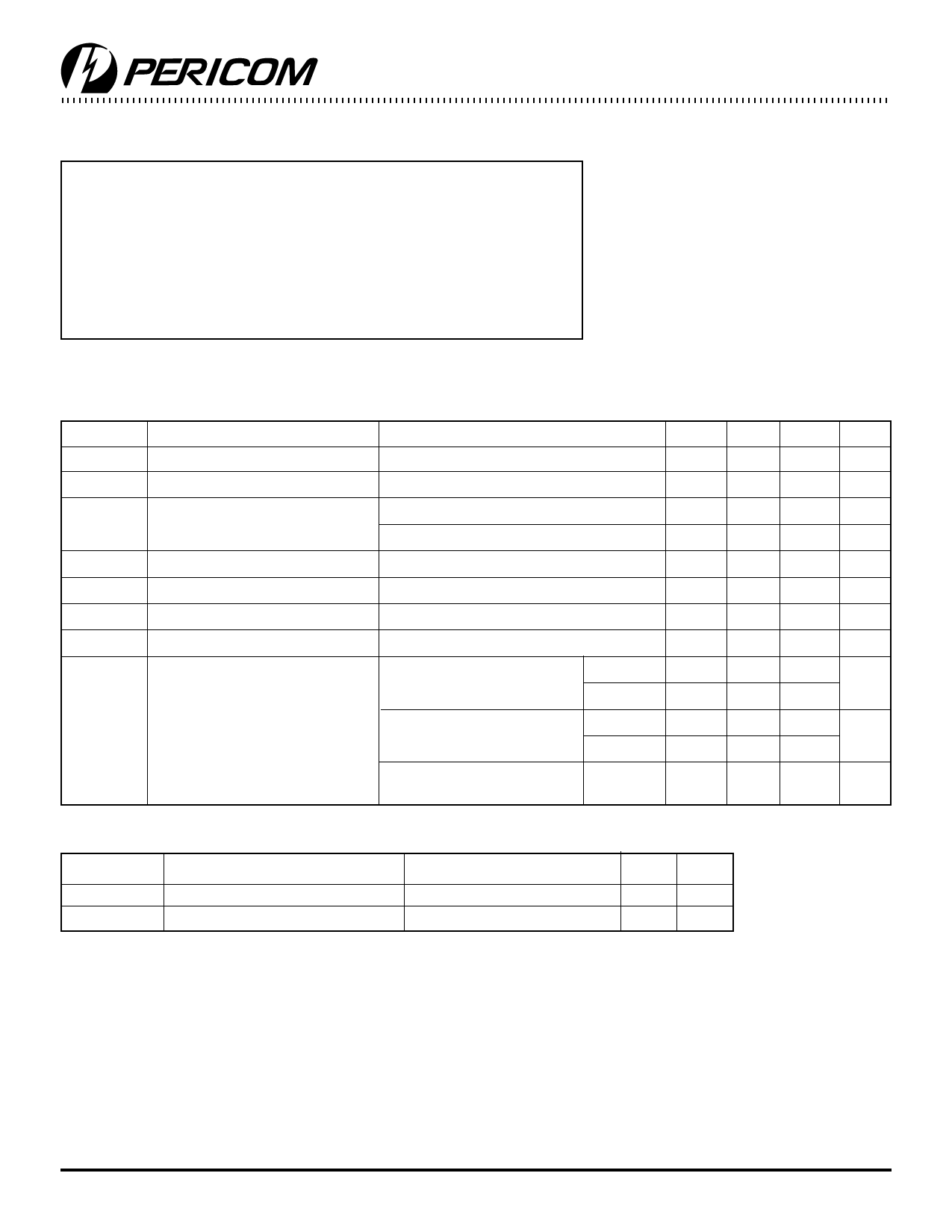
DC Electrical Characteristics (Over the Operating Range, TA = –40°C to +85°C, VCC = 4 to 5V)
Parameters Description
Test Conditions(1)
Min. Typ(2)
VIH
Input HIGH Voltage
Guaranteed Logic HIGH Level
2.0 —
VIL
Input LOW Voltage
Guaranteed Logic LOW Level
–0.5 —
II
Input Current
VCC = 5.5V., VIN = 5.5V OR GND
±1 —
VCC = 0V, VIN = VCC
——
IOZH
High Impedance Output Current 0 ≤ A, B ≤ VCC
——
VIK
Clamp Diode Voltage
VCC = 4.5V, IIN = –18 mA
—
V
IOS
Short Circuit Current(3)
A (B) = 0V, B (A) = VCC
100 —
VH
Input Hysteresis at Control Pins
— 150
RON
Switch On Resistance(4)
VCC = 4.5V, VIN = 0.0V, ION = 30 mA, 64 mA —
5
VCC = 4.5V, VIN = 2.4V, ION = 15 mA
——
VCC = 4 V, VIN = 2.4V, ION = 15 mA
— 14
Max.
—
0.8
—
±1
10
–0.7
—
—
7
15
20
Units
V
V
µA
µA
µA
–1.2
mA
mV
ohm
ohm
ohm
Capacitance (TA = 25°C, f = 1 MHz)
Parameters(5) Description
CIN
COFF
Input Capacitance
A/B Capacitance, Switch Off
Test Conditions
VIN = 0V or 3V
VIN = 0V or 3V
Typ Units
4.5 pF
5.5 pF
Notes:
1. For Max. or Min. conditions, use appropriate value specified under Electrical Characteristics for the applicable device type.
2. Typical values are at Vcc = 5.0V, TA = 25°C ambient and maximum loading.
3. Not more than one output should be shorted at one time. Duration of the test should not exceed one second.
4. Measured by the voltage drop between A and B pin at indicated current through the switch. ON resistance is determined by the
lower of the voltages on the two (A,B) pins.
5. This parameter is determined by device characterization but is not production tested.
2
PS8140A 05/08/02
Share Link: 