M68AW127BL70N6T Ver la hoja de datos (PDF) - STMicroelectronics
Número de pieza
componentes Descripción
Lista de partido
M68AW127BL70N6T Datasheet PDF : 20 Pages
| |||
M68AW127B
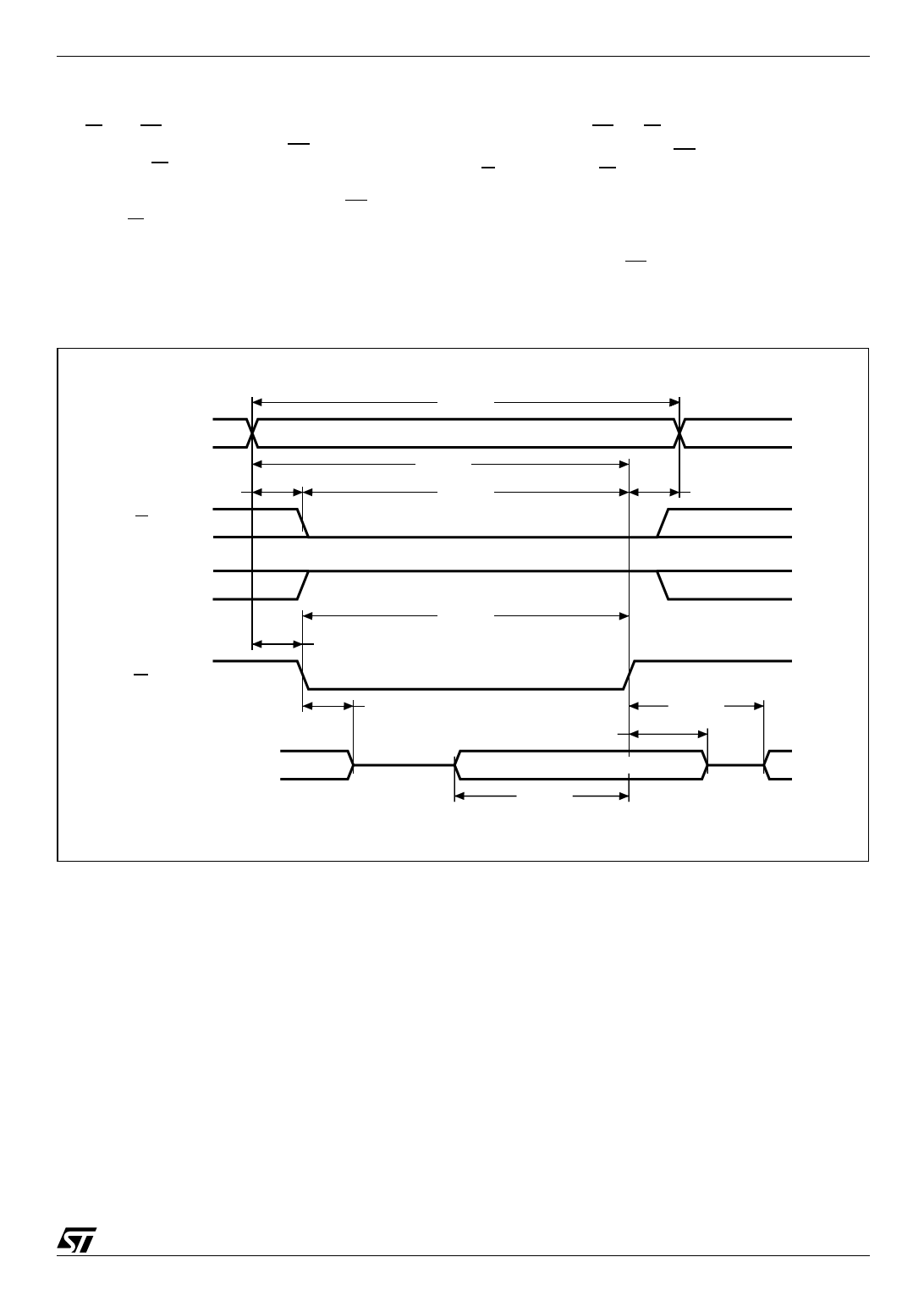
Write Mode
The M68AW127B is in the Write mode whenever
the W and E1 pins are Low and the E2 pin is High.
Either the Chip Enable input (E1) or the Write En-
able input (W) must be de-asserted during Ad-
dress transitions for subsequent write cycles.
Write begins with the concurrence of E1 being ac-
tive with W low. Therefore, address setup time is
referenced to Write Enable and Chip Enable as
tAVWL and tAVEH, respectively, and is determined
by the latter occurring edge.
The Write cycle can be terminated by the earlier
rising edge of E1, or W.
If the Output is enabled (E1 = Low, E2 = High and
G = Low), then W will return the outputs to high im-
pedance within tWLQZ of its falling edge. Care must
be taken to avoid bus contention in this type of op-
eration. Data input must be valid for tDVWH before
the rising edge of Write Enable, or for tDVEH before
the rising edge of E1, whichever occurs first, and
remain valid for tWHDX or tEHDX.
Figure 11. Write Enable Controlled, Write AC Waveforms
A0-A16
tAVEL
E1
E2
W
DQ0-DQ7
tAVAV
VALID
tAVWH
tELWH
tWHAX
tAVWL
tWLWH
tWLQZ
tWHDX
DATA INPUT
tDVWH
tWHQX
AI05478
11/20
Share Link: 