M27W102-100K6TR Ver la hoja de datos (PDF) - STMicroelectronics
Número de pieza
componentes Descripción
Lista de partido
M27W102-100K6TR Datasheet PDF : 15 Pages
| |||
M27W102
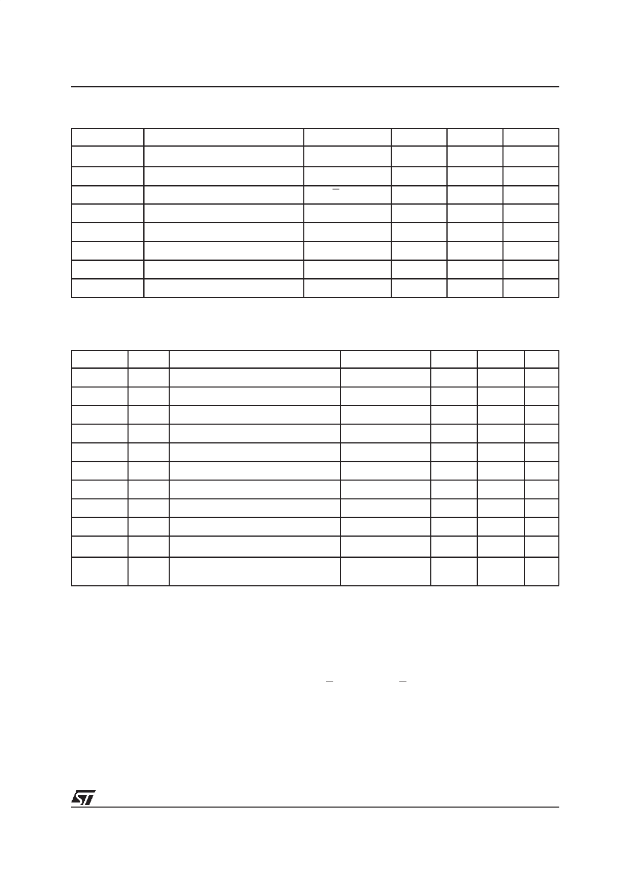
Table 9. Programming Mode AC Characteristics (1)
(TA = 25 °C; VCC = 6.25V ± 0.25V; VPP = 12.75V ± 0.25V)
Symbol
Parameter
Test Condition
Min
Max
ILI
Input Leakage Current
0V ≤ VIN ≤ VIH
±10
ICC
Supply Current
IPP
Program Current
50
E = VIL
50
VIL
Input Low Voltage
VIH
Input High Voltage
–0.3
2
0.8
VCC + 0.5
VOL
Output Low Voltage
VOH
Output High Voltage TTL
IOL = 2.1mA
0.4
IOH = –400µA
2.4
VID
A9 Voltage
11.5
Note: 1. VCC must be applied simultaneously with or before VPP and removed simultaneously or after VPP.
12.5
Unit
µA
mA
mA
V
V
V
V
V
Table 10. Programming Mode AC Characteristics (1)
(TA = 25 °C; VCC = 6.25V ± 0.25V; VPP = 12.75V ± 0.25V)
Symbol
Alt
Parameter
Test Condition
Min
tAVPL
tAS Address Valid to Program Low
2
tQVPL
tDS Input Valid to Program Low
2
tVPHPL
tVPS VPP High to Program Low
2
tVCHPL
tVCS VCC High to Program Low
2
tELPL
tCES Chip Enable Low to Program Low
2
tPLPH
tPW Program Pulse Width
95
tPHQX
tDH Program High to Input Transition
2
tQXGL
tOES Input Transition to Output Enable Low
2
tGLQV
tOE Output Enable Low to Output Valid
tGHQZ (2)
tDFP Output Enable High to Output Hi-Z
0
tGHAX
tAH
Output Enable High to Address
Transition
0
Note: 1. VCC must be applied simultaneously with or before VPP and removed simultaneously or after VPP.
2. Sampled only, not 100% tested.
Max Unit
µs
µs
µs
µs
µs
105
µs
µs
µs
100
ns
130
ns
ns
Programming
The M27W102 has been designed to be fully com-
patible with the M27C1024 and has the same elec-
tronic signature. As a result the M27W102 can be
programmed as the M27C1024 on the same pro-
gramming equipment applying 12.75V on VPP and
6.25V on VCC by the use of the same PRESTO II
algorithm. When delivered (and after each ‘1’s era-
sure for UV EPROM), all bits of the M27W102 are
in the ’1’ state. Data is introduced by selectively
programming ’0’s into the desired bit locations. Al-
though only ’0’s will be programmed, both ’1’s and
’0’s can be present in the data word. The only way
to change a ‘0’ to a ‘1’ is by die exopsure to ultra-
violet light (UV EPROM). The M27W102 is in the
programming mode when VPP input is at 12.75V,
E is at VIL and P is pulsed to VIL. The data to be
programmed is applied to 16 bits in parallel to the
data output pins. The levels required for the ad-
dress and data inputs are TTL. VCC is specified to
be 6.25V ± 0.25V.
7/15
Share Link: 