4244 Ver la hoja de datos (PDF) - Peregrine Semiconductor Corp.
Número de pieza
componentes Descripción
Lista de partido
4244 Datasheet PDF : 6 Pages
| |||
PE4244
Product Specification
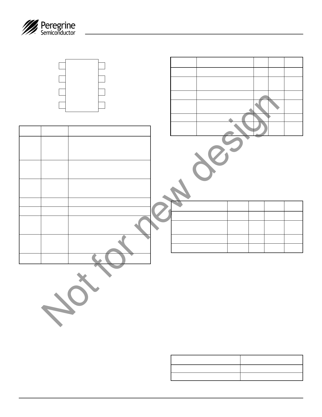
Figure 3. Pin Configuration (Top View)
Table 3. Absolute Maximum Ratings
VDD
1
8 RF1
Symbol
Parameter/Conditions Min Max Units
CTRL 2
4244
7 GND
VDD
Power supply voltage
VI
Voltage on any input
-0.3 4.0
V
-0.3 VDD+
V
GND 3
RFC 4
6 GND
5 RF2
n Table 2. Pin Descriptions
Pin No.
ig 1
s 2
de 3
Pin Name Description
VDD
Nominal 3V supply connection. A bypass
capacitor (100 pF) to the ground plane
should be placed as close as possible to
the pin
CTRL
CMOS logic level:
High = RFC to RF1 signal path
Low = RFC to RF2 signal path
GND
Ground connection. Traces should be
physically short and connected to ground
4
RFC
Common RF port for switch (Note 1)
w 5
RF2
RF2 port (Note 1)
6
GND
Ground Connection. Traces should be
e physically short and connected to ground
n 7
GND
Ground Connection. Traces should be
physically short and connected to ground
r 8
RF1
RF1 port (Note 1)
Note 1: All RF pins must be DC blocked with an external series
fo capacitor or held at 0 VDC
Moisture Sensitivity Level
t The Moisture Sensitivity Level rating for the
No 5x5 mm QFN package is MSL1.
TST
Storage temperature range -65 150
°C
TOP
Operating temperature
-40 85
°C
PIN
VESD
Input power (50Ω)
ESD voltage (Human Body
30
dBm
1500
V
Absolute Maximum Ratings are those values
listed in the above table. Exceeding these values
may cause permanent device damage.
Functional operation should be restricted to the
limits in the DC Electrical Specifications table.
Exposure to absolute maximum ratings for
extended periods may affect device reliability.
Table 4. DC Electrical Specifications
Parameter
VDD Power Supply Voltage
IDD Power Supply Current
VDD = 3V, VCNTL = 3V
Control Voltage High
Control Voltage Low
Min
Typ Max Units
2.7
3.0
3.3
V
250
500
nA
0.7xVDD
V
0.3xVDD
V
Electrostatic Discharge (ESD) Precautions
When handling this UltraCMOS® device, observe
the same precautions that you would use with
other ESD-sensitive devices. Although this device
contains circuitry to protect it from damage due to
ESD, precautions should be taken to avoid
exceeding the specified rating.
Latch-Up Avoidance
Unlike conventional CMOS devices, UltraCMOS®
devices are immune to latch-up.
Table 5. Control Logic Truth Table
Control Voltage
CTRL = CMOS High
CTRL = CMOS Low
Signal Path
RFC to RF1
RFC to RF2
©2005-2013 Peregrine Semiconductor Corp. All rights reserved.
Page 2 of 6
Document No. DOC-30006-2 │ UltraCMOS® RFIC Solutions
Share Link: 