74ACT373(2005) Ver la hoja de datos (PDF) - Fairchild Semiconductor
Número de pieza
componentes Descripción
Lista de partido
74ACT373 Datasheet PDF : 10 Pages
| |||
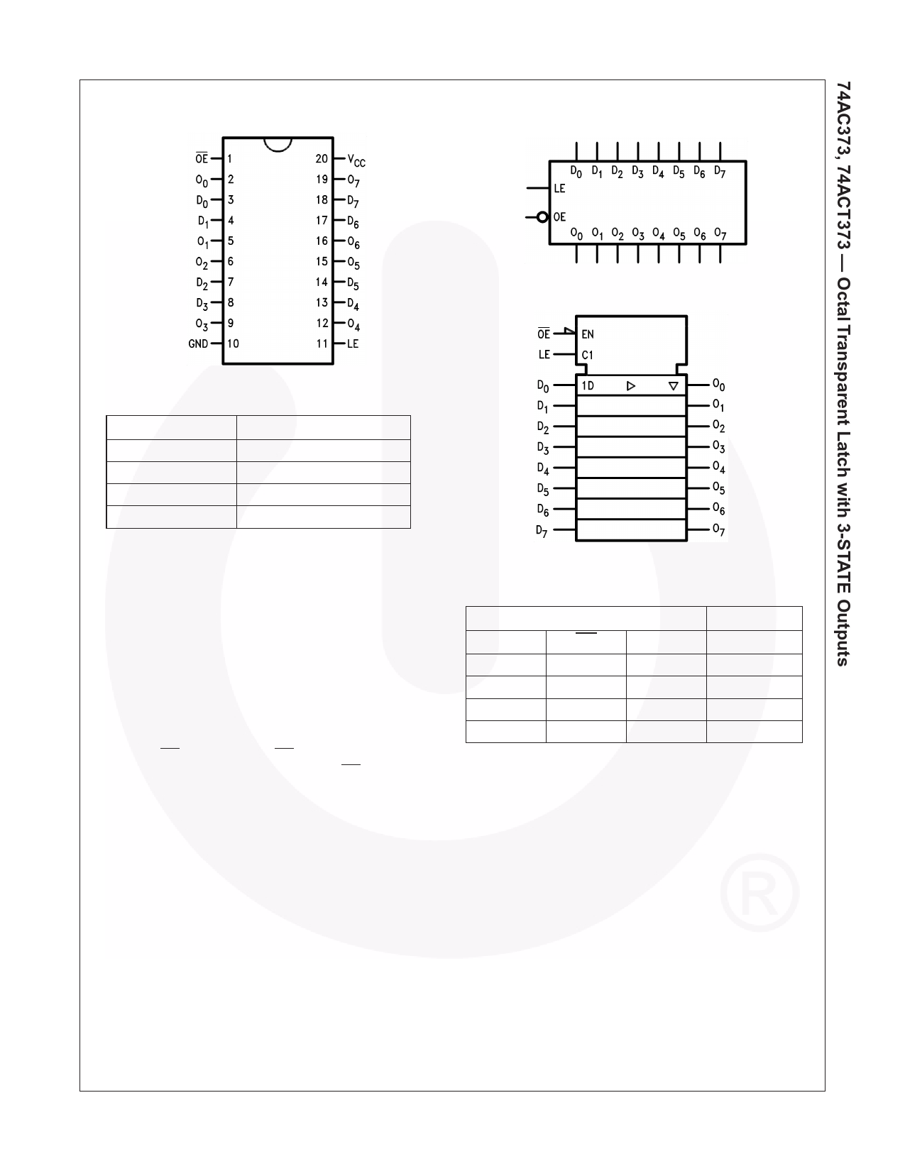
Logic Symbols
IEEE/IEC
Connection Diagram
Logic Diagram
Pin Descriptions
Pin Names
D0–D7
LE
OE
O0–O7
Truth Table
Description
Data Inputs
Latch Enable Input
Output Enable Input
3-STATE Latch Outputs
Inputs
Outputs
LE
OE
Dn
On
X
H
X
Z
H
L
L
L
H
L
H
H
L
L
X
O0
H HIGH Voltage Level
L LOW Voltage Level
Z High Impedance
X Immaterial
O0 Previous O0 before HIGH-to-LOW transition of Latch Enable
Functional Description
The AC/ACT373 contains eight D-type latches with 3-
STATE standard outputs. When the Latch Enable (LE)
input is HIGH, data on the Dn inputs enters the latches. In
this condition the latches are transparent, i.e., a latch out-
put will change state each time its D-type input changes.
When LE is LOW, the latches store the information that
was present on the D-type inputs a setup time preceding
the HIGH-to-LOW transition of LE. The 3-STATE standard
outputs are controlled by the Output Enable (OE) input.
When OE is LOW, the standard outputs are in the 2-state
mode. When OE is HIGH, the standard outputs are in the
high impedance mode but this does not interfere with
entering new data into the latches.
Please note that this diagram is provided only for the understanding of logic operations and should not be used to estimate propagation delays.
www.fairchildsemi.com
2
Share Link: 