MC74ACT241DWR2G Ver la hoja de datos (PDF) - ON Semiconductor
Número de pieza
componentes Descripción
Lista de partido
MC74ACT241DWR2G Datasheet PDF : 8 Pages
| |||
MC74ACT241
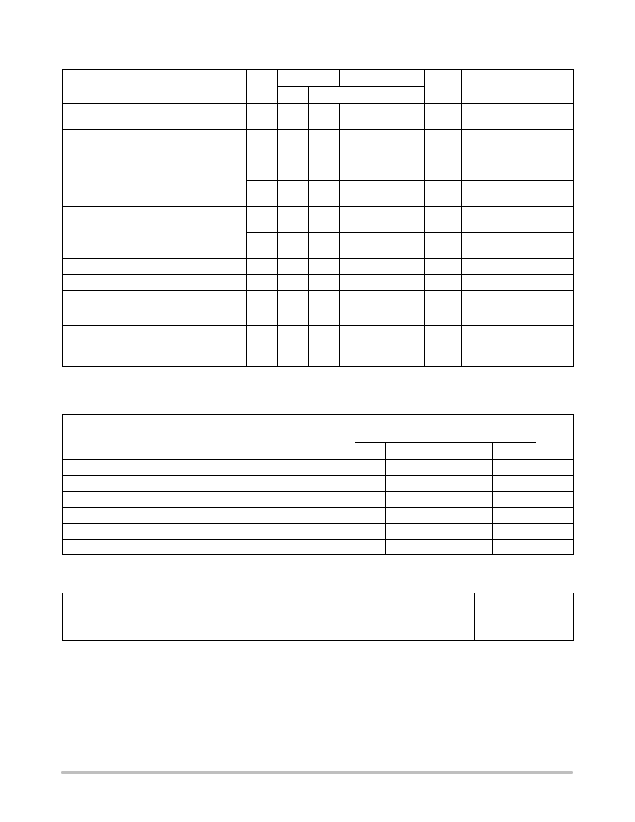
DC CHARACTERISTICS
Symbol
Parameter
VIH
Minimum High Level Input Voltage
VCC
TA = +255C TA = −405C to +855C
(V) Typ
Guaranteed Limits
4.5 1.5 2.0
2.0
5.5 1.5 2.0
2.0
VIL
Maximum Low Level Input Voltage 4.5 1.5 0.8
0.8
5.5 1.5 0.8
0.8
VOH Minimum High Level Output Voltage 4.5 4.49 4.4
4.4
5.5 5.49 5.4
5.4
4.5
− 3.86
3.76
5.5
4.86
4.76
VOL Maximum Low Level Output Voltage 4.5 0.001 0.1
0.1
5.5 0.001 0.1
0.1
4.5
− 0.36
0.44
5.5
0.36
0.44
IIN
Maximum Input Leakage Current
5.5
− ±0.1
±1.0
DICCT Additional Maximum ICC/Input
5.5 0.6
−
1.5
IOZ
Maximum 3−State Current
5.5
− ±0.5
±5.0
IOLD †Minimum Dynamic Output Current 5.5
−
−
75
IOHD
5.5
−75
ICC
Maximum Quiescent Supply Current 5.5
−
8.0
80
*All outputs loaded; thresholds on input associated with output under test.
†Maximum test duration 2.0 ms, one output loaded at a time.
Unit
V
V
V
V
V
V
V
V
V
V
V
V
mA
mA
mA
mA
mA
mA
Conditions
VOUT = 0.1 V or
VCC − 0.1 V
VOUT = 0.1 V or
VCC − 0.1 V
IOUT = −50 mA
*VIN = VIL or VIH −24 mA
IOH
−24 mA
IOUT = 50 mA
*VIN = VIL or VIH 24 mA
IOL
24 mA
VI = VCC, GND
VI = VCC − 2.1 V
VI (OE) = VIL, VIH
VI = VCC, GND
VO = VCC, GND
VOLD = 1.65 V Max
VOHD = 3.85 V Min
VIN = VCC or GND
AC CHARACTERISTICS tr = tf = 3.0 ns (For Figures and Waveforms, See Figures 2, 3, and 4.)
Symbol
Parameter
tPLH Propagation Delay Data to Output
tPHL Propagation Delay Data to Output
tPZH Output Enable Time
tPZL Output Enable Time
tPHZ Output Disable Time
tPLZ Output Disable Time
*Voltage Range 5.0 V is 5.0 V ±0.5 V
TA = +255C
TA = −405C to +855C
VCC*
CL = 50 pF
CL = 50 pF
(V) Min Typ Max
Min
Max
Unit
5.0 1.5 6.5 9.0
1.5
10.0
ns
5.0 1.5 7.0 9.0
1.5
10.0
ns
5.0 1.5 6.0 9.0
1.0
10.0
ns
5.0 1.5 7.0 10.0
1.5
11.0
ns
5.0 1.5 8.0 10.5
1.5
11.5
ns
5.0 2.0 7.0 10.5
1.5
11.5
ns
CAPACITANCE
Symbol
Parameter
CIN
Input Capacitance
CPD Power Dissipation Capacitance
Value Typ Unit
4.5
pF
45
pF
Test Conditions
VCC = 5.0 V
VCC = 5.0 V
http://onsemi.com
3
Share Link: 