7C132-25 Ver la hoja de datos (PDF) - Cypress Semiconductor
Número de pieza
componentes Descripción
Lista de partido
7C132-25 Datasheet PDF : 18 Pages
| |||
CY7C132/CY7C136
CY7C142/CY7C146
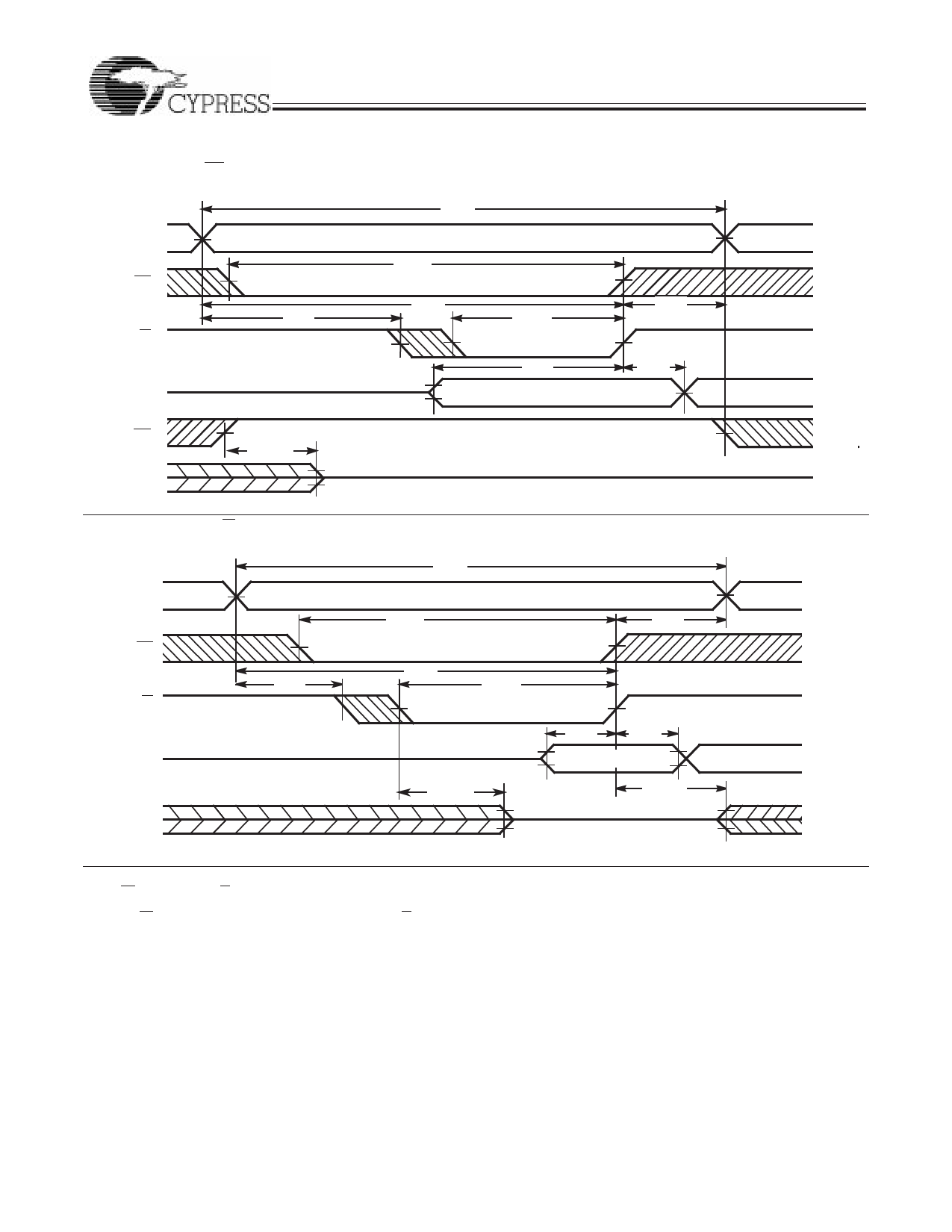
Switching Waveforms (continued)
Write Cycle No.1 (OE Three-States Data I/Os-Either Port)[15, 23]
ADDRESS
CE
R/W
DATAIN
tWC
tSCE
tAW
tSA
tPWE
tSD
DATA VALID
tHA
tHD
OE
DOUT
tHZOE
HIGH IMPEDANCE
Write Cycle No. 2 (R/W Three–States Data I/Os-Either Port)[15, 24]
C132-10
tWC
ADDRESS
tSCE
tHA
CE
R/W
tAW
tSA
tPWE
DATAIN
tSD
tHD
DATA VALID
DOUT
tHZWE
tLZWE
HIGH IMPEDANCE
C132-11
Notes:
23. If OE is LOW during a R/W controlled write cycle, the write pulse width must be the larger of tPWE or tHZWE + tSD to allow the data I/O pins to enter high impedance and for data
to be placed on the bus for the required tSD.
24. If the CE LOW transition occurs simultaneously with or after the R/W LOW transition, the outputs remain in a high-impedance state.
8
Share Link: 