A25L040M Ver la hoja de datos (PDF) - AMIC Technology
Número de pieza
componentes Descripción
Lista de partido
A25L040M Datasheet PDF : 41 Pages
| |||
Read Status Register (RDSR)
The Read Status Register (RDSR) instruction allows the
Status Register to be read. The Status Register may be read
at any time, even while a Program, Erase or Write Status
Register cycle is in progress. When one of these cycles is in
progress, it is recommended to check the Write In Progress
(WIP) bit before sending a new instruction to the device. It is
also possible to read the Status Register continuously, as
shown in Figure 6.
Table 4. Status Register Format
b7 b6
SRWD 0
b5 b4 b3 b2 b1 b0
0 BP2 BP1 BP0 WEL WIP
Status Register
Write Protect
Block Protect Bits
Write Enable Latch Bit
Write In Progress Bit
The status and control bits of the Status Register are as
follows:
WIP bit. The Write In Progress (WIP) bit indicates whether
the memory is busy with a Write Status Register, Program or
Erase cycle. When set to 1, such a cycle is in progress, when
reset to 0 no such cycle is in progress.
A25L016 Series
WEL bit. The Write Enable Latch (WEL) bit indicates the
status of the internal Write Enable Latch. When set to 1 the
internal Write Enable Latch is set, when set to 0 the internal
Write Enable Latch is reset and no Write Status Register,
Program or Erase instruction is accepted.
BP2, BP1, BP0 bits. The Block Protect (BP2, BP1, BP0) bits
are non-volatile. They define the size of the area to be
software protected against Program and Erase instructions.
These bits are written with the Write Status Register (WRSR)
instruction. When one or more of the Block Protect (BP2,
BP1, BP0) bits is set to 1, the relevant memory area (as
defined in Table 1.) becomes protected against Page
Program (PP), Sector Erase (SE), and Block Erase (BE)
instructions. The Block Protect (BP2, BP1, BP0) bits can be
written provided that the Hardware Protected mode has not
been set. The Chip Erase (CE) instruction is executed if, and
only if, all Block Protect (BP2, BP1, BP0) bits are 0.
SRWD bit. The Status Register Write Disable (SRWD) bit is
operated in conjunction with the Write Protect ( W ) signal.
The Status Register Write Disable (SRWD) bit and Write
Protect ( W ) signal allow the device to be put in the
Hardware Protected mode (when the Status Register Write
Disable (SRWD) bit is set to 1, and Write Protect ( W ) is
driven Low). In this mode, the non-volatile bits of the Status
Register (SRWD, TB, BP2, BP1, BP0) become read-only bits
and the Write Status Register (WRSR) instruction is no
longer accepted for execution.
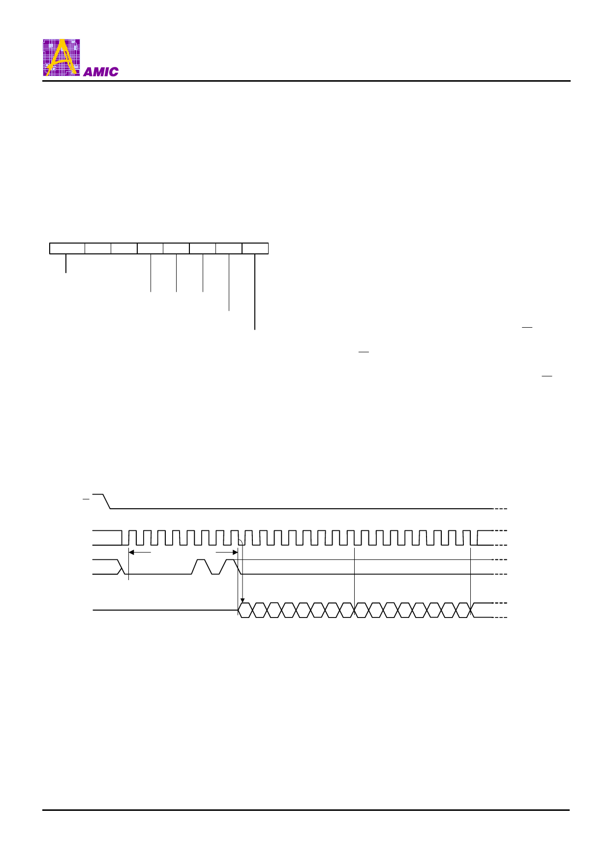
Figure 6. Read Status Register (RDSR) Instruction Sequence and Data-Out Sequence
S
0 1 2 3 4 5 6 7 8 9 10 11 12 13 14 15
C
Instruction
DIO
Status Register Out
Status Register Out
High Impedance
DO
7654 3210765432107
MSB
MSB
(April, 2008, Version 0.0)
12
AMIC Technology Corp.
Share Link: 