A25L040N-F Ver la hoja de datos (PDF) - AMIC Technology
Número de pieza
componentes Descripción
Lista de partido
A25L040N-F Datasheet PDF : 41 Pages
| |||
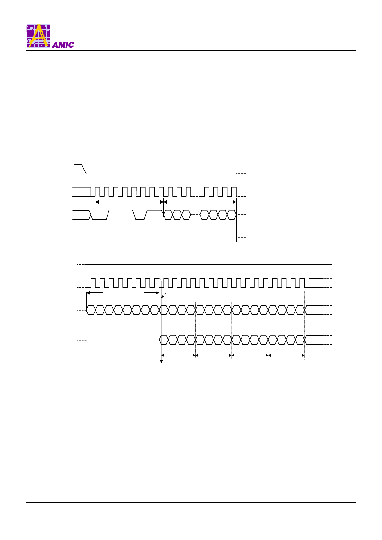
Fast Read Dual Output (3Bh)
The Fast Read Dual Output (3Bh) instruction is similar to the
Fast Read (0Bh) instruction except the data is output on two
pins, DO and DIO, instead of just DO. This allows data to be
transferred from the A25L016 at twice the rate of standard
SPI devices.
Similar to the Fast Read instruction, the Fast Read Dual
Output instruction can operate at the highest possible
frequency of fC (See AC Characteristics). This is
A25L016 Series
accomplished by adding eight “dummy” clocks after the
24-bit address as shown in figure 10. The dummy clocks
allow the device’s internal circuits additional time for setting
up the initial address. The input data during the dummy
clocks is “don’t care”. However, the DIO pin should be
high-impedance prior to the falling edge of the first data out
clock.
Figure 10. FAST_READ_DUAL_OUTPUT Instruction Sequence and Data-Out Sequence
S
0 1 2 3 4 5 6 7 8 9 10 28 29 30 31
C
Instruction
24-Bit Address
DIO
23 22 21 3 2 1 0
MSB
High Impedance
DO
S
32 33 34 35 36 37 38 39 40 41 42 43 44 45 46 47
C
Dummy Byte
DIO switches from input to output
DIO
76543 21 06420642064206420
DO
75 3 1 7 5 3 1 75 3 1 7 5 3 1 7
MSB
Data Out 1
Data Out 2
MSB
Data Out 3
Data Out 4
MSB
Note:. Address bits A23 to A21 are Don’t Care, for A25L016.
(April, 2008, Version 0.0)
17
AMIC Technology Corp.
Share Link: 