A29040V Ver la hoja de datos (PDF) - AMIC Technology
Número de pieza
componentes Descripción
Lista de partido
A29040V Datasheet PDF : 30 Pages
| |||
Write Operation Status
Several bits, I/O2, I/O3, I/O5, I/O6, and I/O7, are provided in
the A29040 to determine the status of a write operation.
Table 5 and the following subsections describe the
functions of these status bits. I/O7, I/O6 and I/O2 each offer
a method for determining whether a program or erase
operation is complete or in progress. These three bits are
discussed first.
I/O7: Data Polling
The Data Polling bit, I/O7, indicates to the host system
whether an Embedded Algorithm is in progress or
completed, or whether the device is in Erase Suspend.
Data Polling is valid after the rising edge of the final WE
pulse in the program or erase command sequence.
During the Embedded Program algorithm, the device
outputs on I/O7 the complement of the datum programmed
to I/O7. This I/O7 status also applies to programming during
Erase Suspend. When the Embedded Program algorithm is
complete, the device outputs the datum programmed to
I/O7. The system must provide the program address to read
valid status information on I/O7. If a program address falls
within a protected sector, Data Polling on I/O7 is active for
approximately 2µs, then the device returns to reading array
data.
During the Embedded Erase algorithm, Data Polling
produces a "0" on I/O7. When the Embedded Erase
algorithm is complete, or if the device enters the Erase
Suspend mode, Data Polling produces a "1" on I/O7.This is
analogous to the complement/true datum output described
for the Embedded Program algorithm: the erase function
changes all the bits in a sector to "1"; prior to this, the
device outputs the "complement," or "0." The system must
provide an address within any of the sectors selected for
erasure to read valid status information on I/O7.
After an erase command sequence is written, if all sectors
selected for erasing are protected, Data Polling on I/O7 is
active for approximately 100µs, then the device returns to
reading array data. If not all selected sectors are protected,
the Embedded Erase algorithm erases the unprotected
sectors, and ignores the selected sectors that are
protected.
When the system detects I/O7 has changed from the
complement to true data, it can read valid data at I/O7 - I/O0
on the following read cycles. This is because I/O7 may
change asynchronously with I/O0 - I/O6 while Output Enable
( OE ) is asserted low. The Data Polling Timings (During
Embedded Algorithms) figure in the "AC Characteristics"
section illustrates this. Table 5 shows the outputs for Data
Polling on I/O7. Figure 3 shows the Data Polling algorithm.
A29040 Series
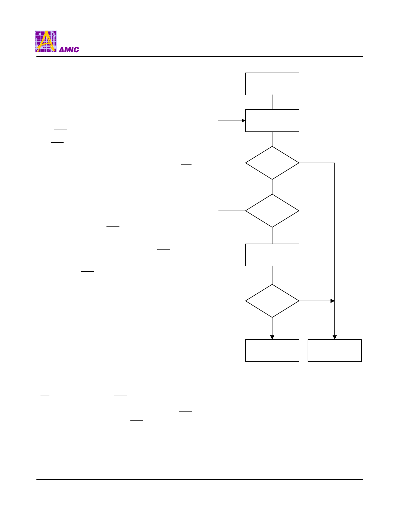
START
Read I/O7-I/O0
Address = VA
Yes
I/O7 = Data ?
No
No
I/O5 = 1?
Yes
Read I/O7 - I/O0
Address = VA
Yes
I/O7 = Data ?
No
FAIL
PASS
Note :
1. VA = Valid address for programming. During a sector
erase operation, a valid address is an address within any
sector selected for erasure. During chip erase, a valid
address is any non-protected sector address.
2. I/O7 should be rechecked even if I/O5 = "1" because
I/O7 may change simultaneously with I/O5.
Figure 3. Data Polling Algorithm
PRELIMINARY (August, 2001, Version 0.5)
11
AMIC Technology, Inc.
Share Link: 