A29DL323UG-90(2002) Ver la hoja de datos (PDF) - AMIC Technology
Número de pieza
componentes Descripción
Lista de partido
A29DL323UG-90
(Rev.:2002)
(Rev.:2002)
AMIC Technology

A29DL323UG-90 Datasheet PDF : 46 Pages
| |||
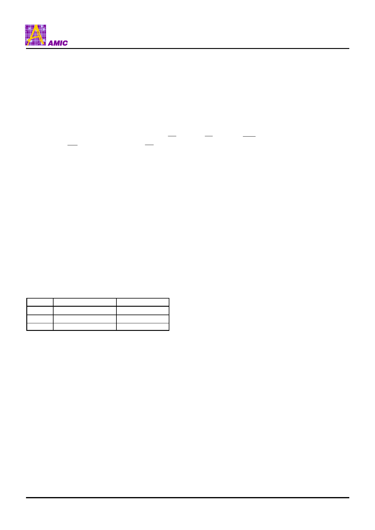
Block Diagram
VCC
GND
A0-A20
Address
Buffers
Bank 2 Address
WP(ACC)
RESET
WE
BYTE
CE
OE
Bank / Sector
Decoder
State
Control
(Command
Register)
Program / Erase
Voltage Generator
A29DL323 Series
X-Decoder
Cell Matrix
(Bank 2)
Y-Decoder
Y-Gating
SA / WC
Data Latch
SA / WC
I/O0 - I/O 15 (A-1)
Input / Output
Buffers
RY/BY
Bank 1 Address
Y-Decoder
Y-Gating
X-Decoder
Cell Matrix
(Bank 1)
Pin Descriptions
Pin No.
A0 – A20
I/O0 - I/O14
I/O15 (A-1)
I/O15
A-1
CE
WE
OE
RESET
BYTE
RY/ BY
WP (ACC)
GND
VCC
NC Note
Description
Address Inputs
Data Inputs/Outputs
Data Input/Output, Word Mode
LSB Address Input, Byte Mode
Chip Enable
Write Enable
Output Enable
Hardware Reset Input
Mode Select
Ready/ BUSY - Output
Write Protect (Accelerated) Input
Ground
Power Supply
No Connection
Note: Some signals can be applied because this pin is not connected to the inside of the chip.
PRELIMINARY (May, 2002, Version 0.0)
3
AMIC Technology, Inc.
Share Link: