A29DL324UV-80 Ver la hoja de datos (PDF) - AMIC Technology
Número de pieza
componentes Descripción
Lista de partido
A29DL324UV-80
AMIC Technology

A29DL324UV-80 Datasheet PDF : 50 Pages
| |||
A29DL32x Series
Hardware Data Protection
The command sequence requirement of unlock cycles for
programming or erasing provides data protection against
inadvertent writes (refer to Table 12 for command definitions).
In addition, the following hardware data protection measures
prevent accidental erasure or programming, which might
otherwise be caused by spurious system level signals during
VCC power-up and power-down transitions, or from system
noise.
Low VCC Write Inhibit
When VCC is less than VLKO, the device does not accept any
write cycles. This protects data during VCC power-up and
power-down. The command register and all internal
program/erase circuits are disabled, and the device resets to
reading array data. Subsequent writes are ignored until VCC
is greater than VLKO. The system must provide the proper
signals to the control pins to prevent unintentional writes
when VCC is greater than VLKO.
Write Pulse “Glitch” Protection
Noise pulses of less than 5ns (typical) on OE , CE or WE
do not initiate a write cycle.
Logical Inhibit
Write cycles are inhibited by holding any one of OE = VIL,
CE = VIH or WE = VIH. To initiate a write cycle, CE and
WE must be a logical zero while OE is a logical one.
Power-Up Write Inhibit
If WE = CE = VIL and OE = VIH during power up, the
device does not accept commands on the rising edge of WE .
The internal state machine is automatically reset to reading
array data on power-up.
COMMON FLASH MEMORY INTERFACE (CFI)
The Common Flash Interface (CFI) specification outlines
device and host system software interrogation handshake,
which allows specific vendor-specified software algorithms to
be used for entire families of devices. Software support can
then be device-independent, JEDEC ID-independent, and
forward- and backward-compatible for the specified flash
device families. Flash vendors can standardize their existing
interfaces for long-term compatibility.
This device enters the CFI Query mode when the system
writes the CFI Query command, 98h, to address 55h in word
mode (or address AAh in byte mode), any time the device is
ready to read array data. The system can read CFI
information at the addresses given in Tables 8-11. To
terminate reading CFI data, the system must write the reset
command.
The system can also write the CFI query command when the
device is in the autoselect mode. The device enters the CFI
query mode, and the system can read CFI data at the
addresses given in Tables 8-11. The system must write the
reset command to return the device to the autoselect mode.
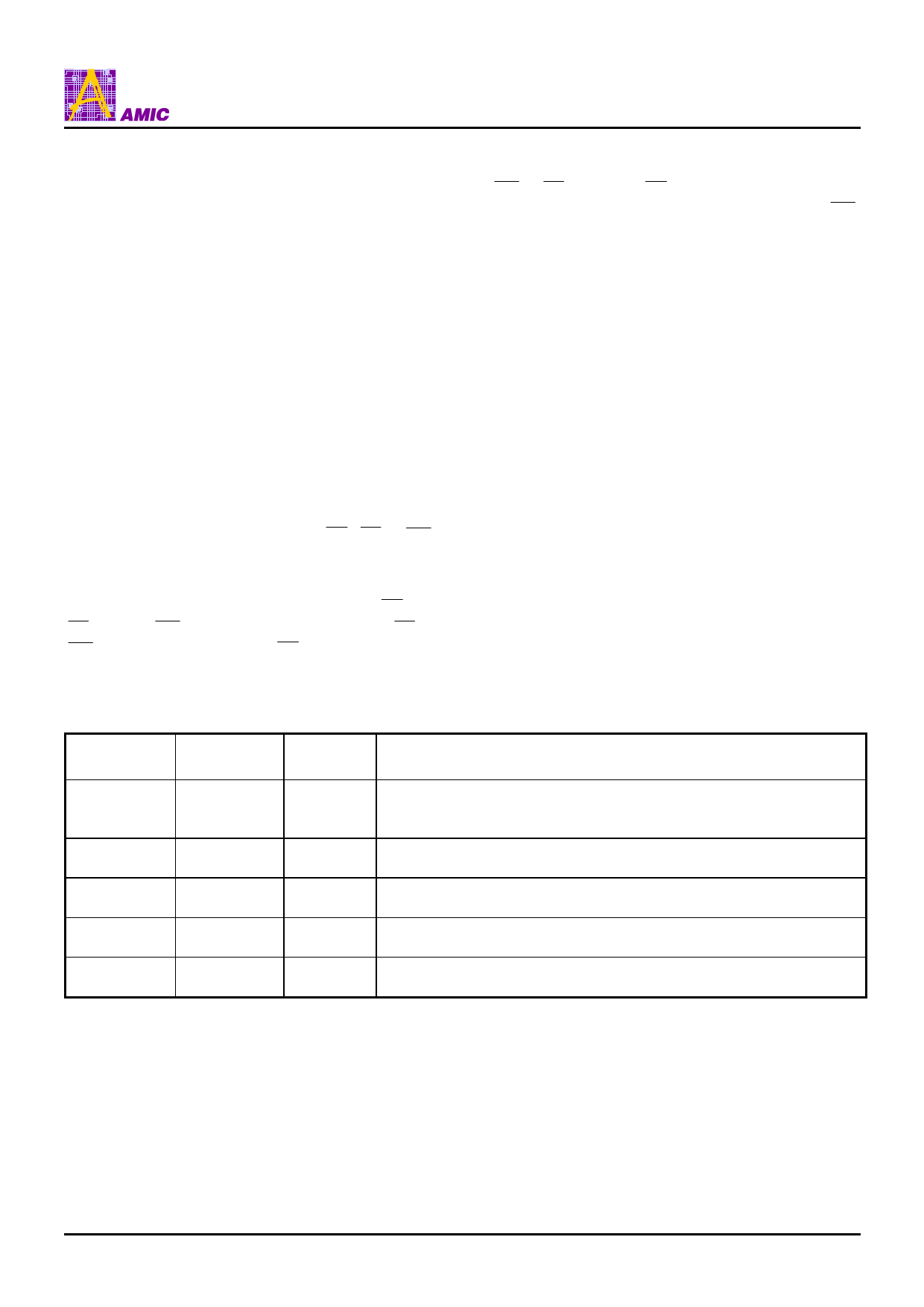
Addresses
(Word Mode)
10h
11h
12h
13h
14h
15h
16h
17h
18h
19h
1Ah
Addresses
(Byte Mode)
20h
22h
24h
26h
28h
2Ah
2Ch
2Eh
30h
32h
34h
Table 8. CFI Query Identification String
Data
0051h
0052h
0059h
0002h
0000h
0040h
0000h
0000h
0000h
0000h
0000h
Description
Query Unique ASCII string “QRY”
Primary OEM Command Set
Address for Primary Extended Table
Alternate OEM Command Set (00h = none exists)
Address for Alternate OEM Extended Table (00h = none exists)
PRELIMINARY (May, 2005, Version 0.0)
18
AMIC Technology, Corp.
Share Link: