A45L9332AF Ver la hoja de datos (PDF) - AMIC Technology
Número de pieza
componentes Descripción
Lista de partido
A45L9332AF Datasheet PDF : 55 Pages
| |||
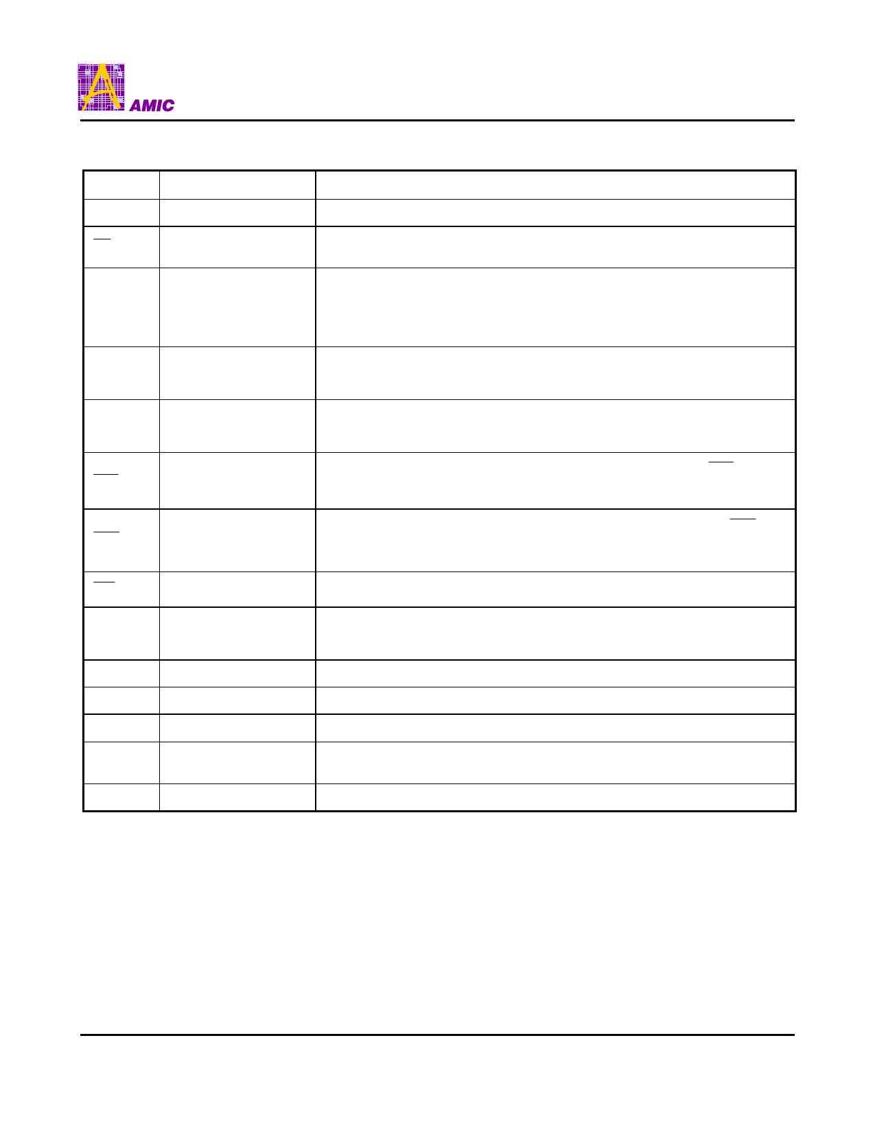
A45L9332A Series
Pin Descriptions
Symbol
CLK
Name
System Clock
CS
Chip Select
CKE
Clock Enable
A0~A9
Address
A10(BA) Bank Select Address
RAS
Row Address Strobe
Description
Active on the positive going edge to sample all inputs.
Disables or Enables device operation by masking or enabling all inputs except
CLK, CKE and DQMi
Masks system clock to freeze operation from the next clock cycle.
CKE should be enabled at least one clock + t ss prior to new command.
Disable input buffers for power down in standby.
Row / Column addresses are multiplexed on the same pins.
Row address : RA0~RA9, Column address: CA0~CA7
Selects bank to be activated during row address latch time.
Selects band for read/write during column address latch time.
Latches row addresses on the positive going edge of the CLK with RAS low.
Enables row access & precharge.
CAS
Latches column addresses on the positive going edge of the CLK with CAS low.
Column Address Strobe
Enables column access.
WE
Write Enable
Enables write operation and Row precharge.
DQMi
Makes data output Hi-Z, t SHZ after the clock and masks the output.
Data Input/Output Mask
Blocks data input when DQM active. (Byte Masking)
DQi
Data Input/Output
Data inputs/outputs are multiplexed on the same pins.
DSF
Define Special Function Enables write per bit, block write and special mode register set.
VDD/VSS Power Supply/Ground Power Supply: +3.3V±0.3V/Ground
VDDQ/VS Data Output
SQ
Power/Ground
Provide isolated Power/Ground to DQs for improved noise immunity.
NC
No Connection
PRELIMINARY (October, 2001, Version 0.1)
4
AMIC Technology, Inc.
Share Link: 