GS88237BB-225I Ver la hoja de datos (PDF) - Giga Semiconductor
Número de pieza
componentes Descripción
Lista de partido
GS88237BB-225I Datasheet PDF : 26 Pages
| |||
Preliminary
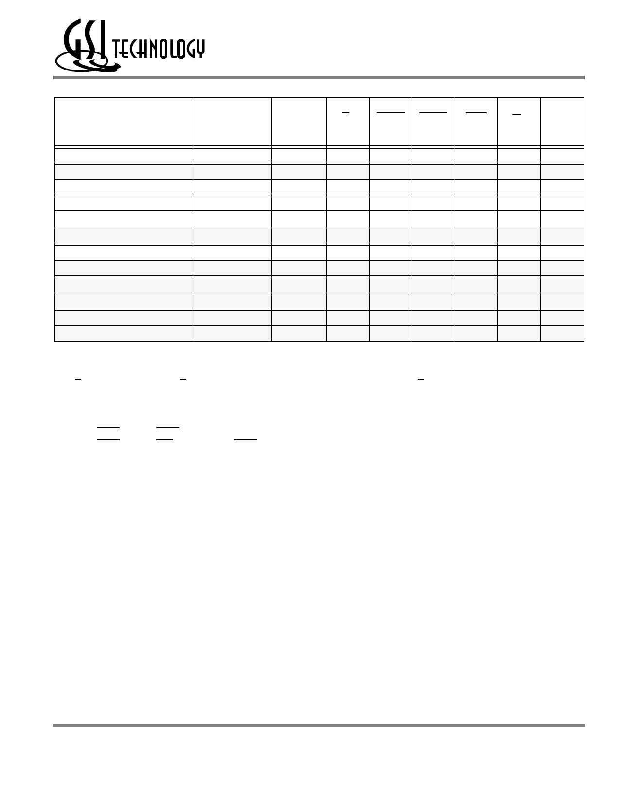
GS88237BB-333/300/275/250/225/200
Synchronous Truth Table
Operation
State
Address Used Diagram E1 ADSP ADSC ADV W3 DQ4
Key5
Deselect Cycle, Power Down
None
X
H
X
L
X
X
High-Z
Read Cycle, Begin Burst
External
R
L
L
X
X
X
Q
Read Cycle, Begin Burst
External
R
L
H
L
X
F
Q
Write Cycle, Begin Burst
External
W
L
H
L
X
T
D
Read Cycle, Continue Burst
Next
CR
X
H
H
L
F
Q
Read Cycle, Continue Burst
Next
CR
H
X
H
L
F
Q
Write Cycle, Continue Burst
Next
CW
X
H
H
L
T
D
Write Cycle, Continue Burst
Next
CW
H
X
H
L
T
D
Read Cycle, Suspend Burst
Current
X
H
H
H
F
Q
Read Cycle, Suspend Burst
Current
H
X
H
H
F
Q
Write Cycle, Suspend Burst
Current
X
H
H
H
T
D
Write Cycle, Suspend Burst
Current
H
X
H
H
T
D
Notes:
1. X = Don’t Care, H = High, L = Low
2. W = T (True) and F (False) is defined in the Byte Write Truth Table preceding
3. G is an asynchronous input. G can be driven high at any time to disable active output drivers. G low can only enable active drivers (shown
as “Q” in the Truth Table above).
4. All input combinations shown above are tested and supported. Input combinations shown in gray boxes need not be used to accomplish
basic synchronous or synchronous burst operations and may be avoided for simplicity.
5. Tying ADSP high and ADSC low allows simple non-burst synchronous operations. See BOLD items above.
6. Tying ADSP high and ADV low while using ADSC to load new addresses allows simple burst operations. See ITALIC items above.
Rev: 1.00b 12/2002
7/26
© 2002, Giga Semiconductor, Inc.
Specifications cited are subject to change without notice. For latest documentation see http://www.gsitechnology.com.
Share Link: 