ACT4082AUS-T Ver la hoja de datos (PDF) - Active-Semi, Inc
Número de pieza
componentes Descripción
Lista de partido
ACT4082AUS-T Datasheet PDF : 11 Pages
| |||
Active-Semi
ACT4082A
Rev0, 16-May-08
ORDERING INFORMATION
PART NUMBER TEMPERATURE RANGE
ACT4082AUS-T
-40°C to 85°C
PACKAGE
SOT23-6
PINS
6
PACKING TOP MARK
TAPE & REEL
FMGD
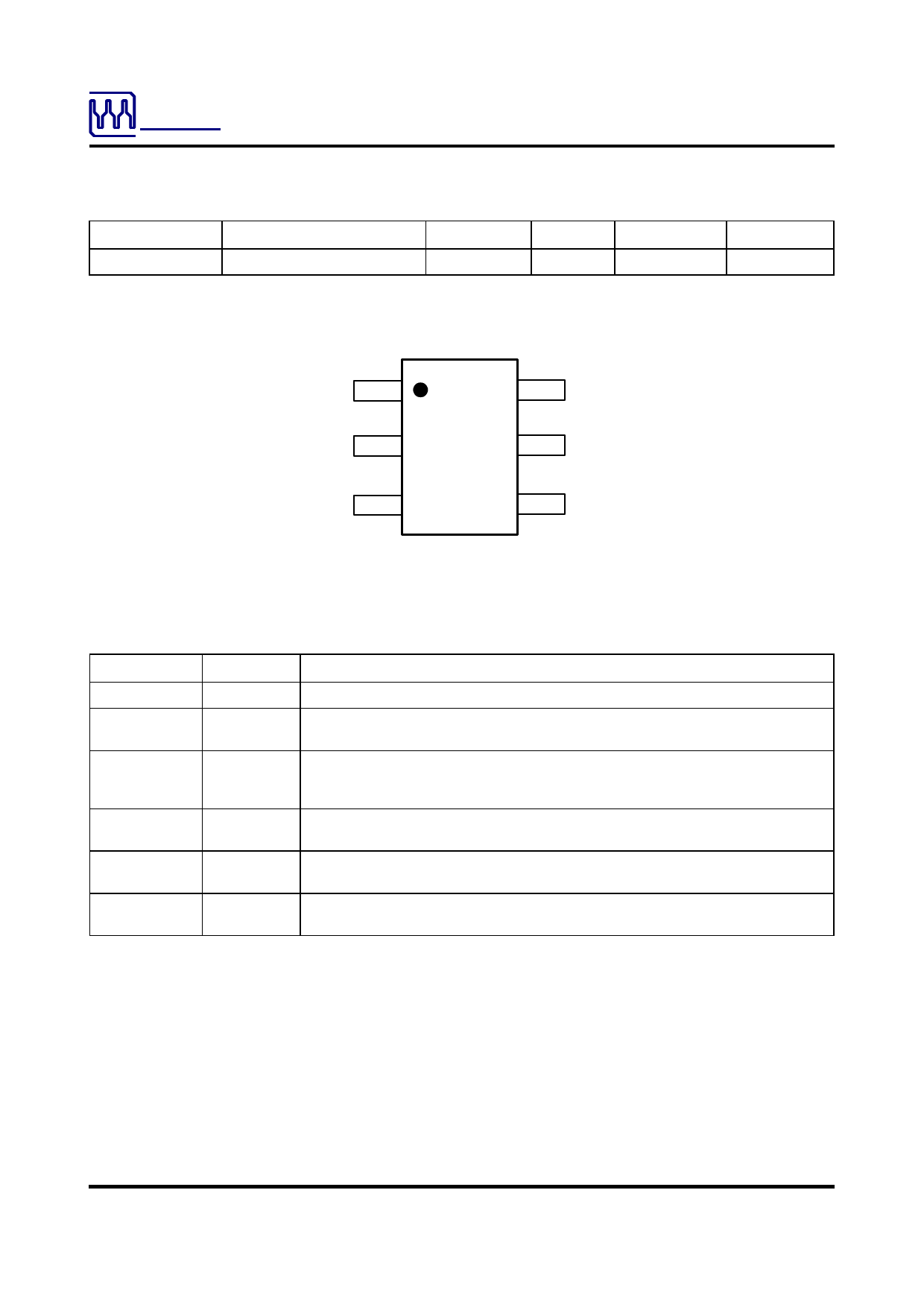
PIN CONFIGURATION
SW 1
6 BST
IN 2 ACT4082A 5 G
EN 3
4 FB
SOT23-6
PIN DESCRIPTIONS
PIN NUMBER PIN NAME
PIN DESCRIPTION
1
SW
Switch Output. Connect this pin to the switching end of the inductor.
2
IN
Power supply input. Bypass this pin with a 10µF ceramic capacitor to G, placed as
close to the IC as possible.
Enable Input. EN is pulled up to 5V with a 2µA current, and contains a precise 1.24V
3
EN
logic threshold. Drive this pin to a logic-high or leave unconnected to enable the IC.
Drive to a logic-low to disable the IC and enter micro-power shutdown mode.
4
FB
Feedback Input. The voltage at this pin is regulated to 0.81V. Connect to the center
point of a resistive voltage-divider between OUT and G to set the output voltage.
5
G
Ground and Heat sink. Connect this pin to a large, uncovered PCB copper area for
best heat dissipation.
6
BST
Bootstrap. This pin acts as the power supply for the high-side switch’s gate driver.
Connect a 22nF capacitor between this pin and SW.
Innovative PowerTM
-2-
www.active-semi.com
Copyright © 2008 Active-Semi, Inc.
Share Link: 