ACT6391 Ver la hoja de datos (PDF) - Active-Semi, Inc
Número de pieza
componentes Descripción
Lista de partido
ACT6391 Datasheet PDF : 12 Pages
| |||
ACT6390/ACT6391
Rev 1, 22-Aug-13
Inductor Selection
As a step-up converter, the switch duty cycle (D) is
determined by the input voltage (VIN) and output
voltage (VOUT), as given by the following formula:
D = VOUT − VIN
(3)
VOUT
Define
K = ΔIL
IL(DC )
(4)
Where: ∆IL is the inductor ripple current in steady
state, typically chosen to be about 0.3, and
ΔIL
= VIN
L
DT
= VIN × D
L × fSW
(5)
IL(DC) is the inductor DC current, given by:
IL (DC )
=
VOUT × IOUT
VIN × η
(6)
Where η is typical efficiency.
Solving equations (3),(4),(5) and (6) for the inductor
value,
( ) L = ⎜⎜⎝⎛VVOIUNT ⎟⎟⎠⎞2
VOUT −VIN
IOUT × fSW
×η
K
(7)
This equation can be used to determine the correct
trade-off between efficiency, current ripple, size and
cost.
When selecting an inductor make sure that the in-
ductors maximum DC current and saturation current
exceed the maximum operation point, calculated
by:
IL(DC ,MAX )
=
IOUT (MAX ) ×VOUT
VIN (MIN ) × η
(8)
and
IL(PEAK,MAX )
= IL(DC,MAX )
+1
2
ΔIL(MAX )
[ ] = IOUT (MAX ) ×VOUT + 1 ×VIN(MIN) VOUT −VIN(MIN)
VIN(MIN) × η
2
VOUT × L ×fSW
(9)
If the output voltage is greater than two times of
input voltage, that means the duty cycle is greater
than 50%, the slope compensation is required for
stability. When operating in this condition ensure
that the inductor value is greater than LMIN:
( ) L > LMIN
=
VOUT −VIN × RCS
1.75 × fSW
(10)
Where RCS is the current sense trans-resistance,
RCS is 0.45Ω for ACT6390, and RCS = 0.3Ω for
ACT6391.
For example: VIN = 3.3V, VOUT = 12V, fSW = 700kHz
IOUT = 250mA, η = 85%, FREQ = G, K = 0.4
L
=
⎜⎜⎝⎛
VIN
VOUT
⎟⎟⎠⎞2
⎜⎜⎝⎛
VOUT
IOUT
−VIN
× fSW
⎟⎟⎠⎞ ×
η
K
(11)
= ⎜⎛ 3.3V ⎟⎞2 ⎜⎛ 12V − 3.3V × 0.85 ⎟⎞ ≈ 7.99μH
⎝ 12V ⎠ ⎝ 250mA×700kHz 0.4 ⎠
Select L = 10µH
Assuming the minimum input voltage is 3V and low
cost external components are used, yielding a low
efficiency of just 80%.
IL(DC,MAX )
=
250mA ×12V
3V × 0.8
= 1.25A
ΔIL(MAX )
=
3V × (12V − 3V )
12V ×10 μH ×700kHz
=
0.32 A
(12)
(13)
IPEAK(MAX )
=
1.25
A
+
1
2
0.32 A
=
1.41A
(14)
For stability,
LMIN
=
(12V − 3.3V )× 0.45Ω
1.75 ×700kHz
=
3.2 μH
(15)
Which meets the slope compensation requirement.
Loop Compensation
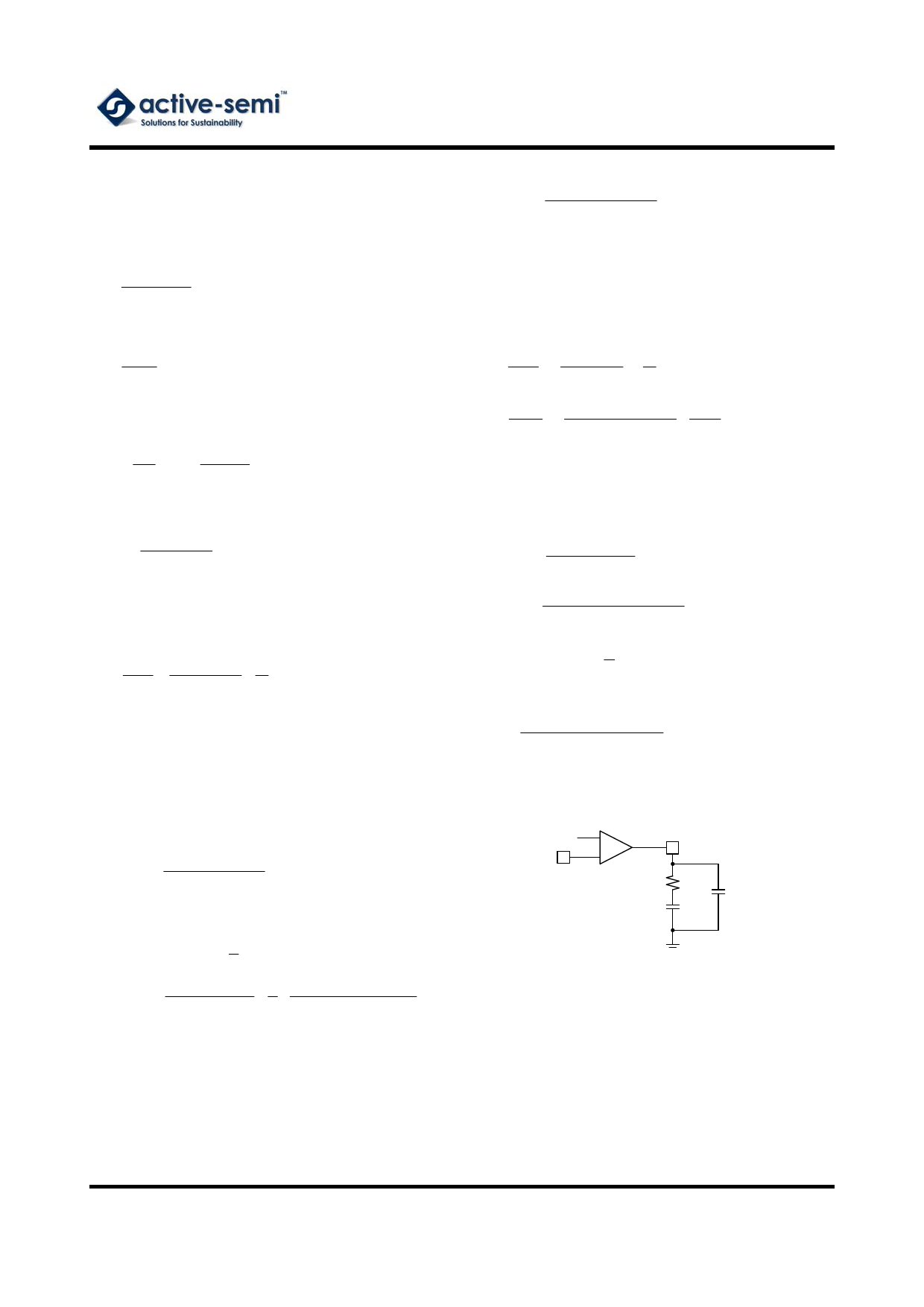
REF
FB 2
+
GM
EA
-
COMP
3
RCOMP
CCOMP
CCOMP2
The ACT6390 and ACT6391 feature a simple loop
compensation scheme. Simple follow the procedure
detailed below to determine suitable compensation
components. For best results be sure to prototype
to confirm the values, and adjust the compensation
network (by inspecting the transient response, for
example) as needed to optimize results for your
particular application.
When the converter operates with continuous in-
ductor current, a right-half-plane zero exits in the
loop’s gain-frequency response. To ensure stability,
Innovative PowerTM
-6-
www.active-semi.com
Copyright © 2013 Active-Semi, Inc.
Share Link: 