AD7490BCPZ-REEL7 Ver la hoja de datos (PDF) - Analog Devices
Número de pieza
componentes Descripción
Lista de partido
AD7490BCPZ-REEL7 Datasheet PDF : 29 Pages
| |||
Data Sheet
AD7490
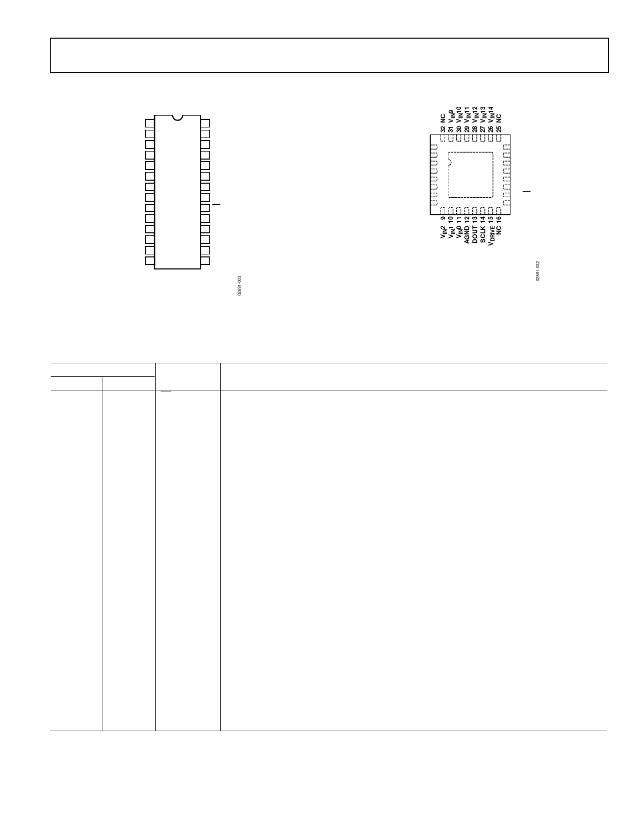
PIN CONFIGURATIONS AND FUNCTION DESCRIPTIONS
VIN11 1
28 VIN12
VIN10 2
27 VIN13
VIN9 3
26 VIN14
NC 4
25 VIN15
VIN8 5
VIN7 6
AD7490
TOP VIEW
24 AGND
23 REFIN
VIN6 7 (Not to Scale) 22 VDD
VIN5 8
21 AGND
VIN4 9
20 CS
VIN3 10
19 DIN
VIN2 11
18 NC
VIN1 12
17 VDRIVE
VIN0 13
16 SCLK
AGND 14
15 DOUT
NC = NO CONNECT
ALL NC PINS SHOULD BE
CONNECTED STRAIGHT TO AGND
Figure 3. 28-Lead TSSOP Pin Configuration
NC 1
VIN8 2
VIN7 3
VIN6 4
VIN5 5
VIN4 6
VIN3 7
NC 8
AD7490
TOP VIEW
(Not to Scale)
24 VIN15
23 NC
22 AGND
21 REFIN
20 VDD
19 AGND
18 CS
17 DIN
NOTES
1. NC = NO CONNECT. ALL NC PINS
SHOULD BE CONNECTED STRAIGHT
TO AGND.
2. CONNECT EXPOSED PAD TO GND
Figure 4. 32-Lead LFCSP Pin Configuration
Table 4. Pin Function Descriptions
Pin No.
TSSOP LFCSP
Mnemonic
20
18
CS
23
21
REFIN
22
20
VDD
14, 21, 24 12, 19, 22 AGND
13 to 5,
3 to 1,
28 to 25
11 to 9,
7 to 2,
31 to 26,
24
VIN0 to VIN15
19
17
DIN
15
13
DOUT
16
14
17
15
N/A
EP
SCLK
VDRIVE
EPAD
Description
Chip Select. Active low logic input. This input provides the dual function of initiating
conversions on the AD7490 and also frames the serial data transfer.
Reference Input for the AD7490. An external reference must be applied to this input. The
voltage range for the external reference is 2.5 V ± 1% for specified performance.
Power Supply Input. The VDD range for the AD7490 is from 2.7 V to 5.25 V. For the 0 V to 2 × REFIN
range, VDD should be from 4.75 V to 5.25 V.
Analog Ground. Ground reference point for all circuitry on the AD7490. All analog/digital input
signals and any external reference signal should be referred to this AGND voltage. All AGND pins
should be connected together.
Analog Input 0 through Analog Input 15. Sixteen single-ended analog input channels that are
multiplexed into the on chip track-and-hold. The analog input channel to be converted is
selected by using the address bits ADD3 through ADD0 of the control register. The address bits,
in conjunction with the SEQ and SHADOW bits, allow the sequence register to be programmed.
The input range for all input channels can extend from 0 V to REFIN or 0 V to 2 × REFIN as selected
via the RANGE bit in the control register. Any unused input channels should be connected to
AGND to avoid noise pickup.
Data In. Logic input. Data to be written to the control register of the AD7490 is provided on this
input and is clocked into the register on the falling edge of SCLK (see the Control Register
section).
Data Out. Logic output. The conversion result from the AD7490 is provided on this output as a
serial data stream. The bits are clocked out on the falling edge of the SCLK input. The data
stream consists of four address bits indicating which channel the conversion result corresponds
to, followed by the 12 bits of conversion data, which is provided by MSB first. The output coding
can be selected as straight binary or twos complement via the CODING bit in the control
register.
Serial Clock. Logic input. SCLK provides the serial clock for accessing data from the part. This
clock input is also used as the clock source for the conversion process of the AD7490.
Logic Power Supply Input. The voltage supplied at this pin determines at what voltage the serial
interface of the AD7490 operates.
Exposed Pad. Connect exposed pad to GND.
Rev. D | Page 7 of 28
Share Link: 