EV-ADF4159EB2Z Ver la hoja de datos (PDF) - Analog Devices
Número de pieza
componentes Descripción
Lista de partido
EV-ADF4159EB2Z
Analog Devices

EV-ADF4159EB2Z Datasheet PDF : 36 Pages
| |||
ADF4159
Data Sheet
Parameter1
NOISE CHARACTERISTICS
Normalized Phase Noise Floor3
Integer-N Mode
Fractional-N Mode
Normalized 1/f Noise (PN1_f)4
Phase Noise Performance5
12,002 MHz Output6
Min
Typ
Max
Unit
Test Conditions/Comments
−224
−217
−120
−96
dBc/Hz
dBc/Hz
dBc/Hz
dBc/Hz
PLL loop BW = 1 MHz
FRAC = 0
Measured at 10 kHz offset, normalized
to 1 GHz
At VCO output
At 50 kHz offset, 100 MHz PFD frequency
1 Operating temperature: −40°C to +125°C.
2 Guaranteed by design. Sample tested to ensure compliance.
3 This specification can be used to calculate phase noise for any application. Use the formula ((Normalized Phase Noise Floor) + 10 log(fPFD) + 20 logN) to calculate
in-band phase noise performance as seen at the VCO output.
4 The PLL phase noise is composed of flicker (1/f) noise plus the normalized PLL noise floor. The formula for calculating the 1/f noise contribution at an RF frequency (fRF)
and at an offset frequency (f) is given by PN = PN1_f + 10 log(10 kHz/f) + 20 log(fRF/1 GHz). Both the normalized phase noise floor and flicker noise are modeled in ADIsimPLL.
5 The phase noise is measured with the EV-ADF4159EB3Z and the Rohde & Schwarz FSUP signal source analyzer.
6 fREFIN = 100 MHz; fPFD = 100 MHz; offset frequency = 50 kHz; RFOUT = 12,002 MHz; N = 120.02; loop bandwidth = 250 kHz.
TIMING SPECIFICATIONS
AVDD = VP = 2.7 V to 3.45 V, DVDD = SDVDD = 1.8 V, AGND = DGND = SDGND = CPGND = 0 V, TA = TMIN to TMAX, dBm referred to 50 Ω,
unless otherwise noted.
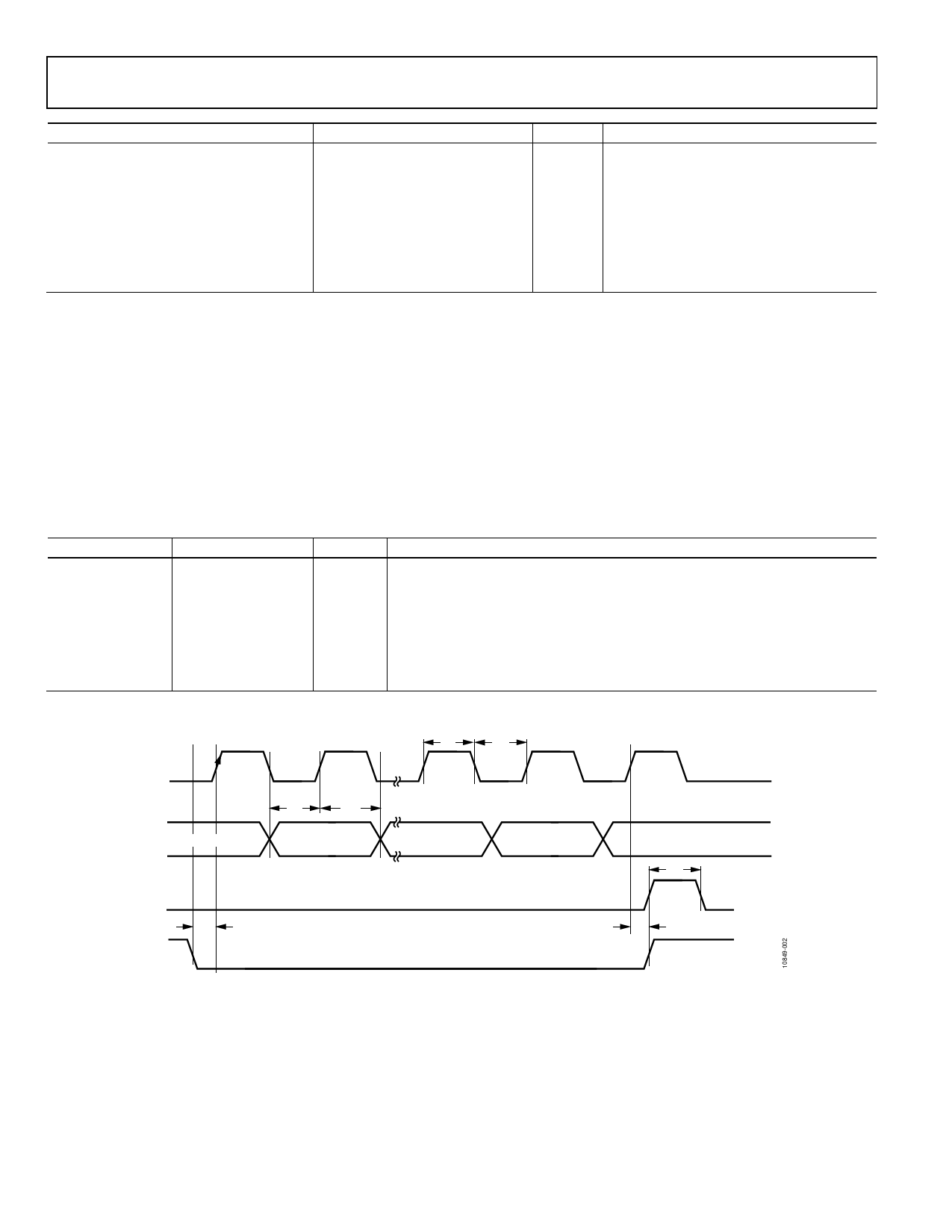
Table 2. Write Timing
Parameter
Limit at TMIN to TMAX
t1
20
t2
10
t3
10
t4
25
t5
25
t6
10
t7
20
Unit
ns min
ns min
ns min
ns min
ns min
ns min
ns min
Description
LE setup time
DATA to CLK setup time
DATA to CLK hold time
CLK high duration
CLK low duration
CLK to LE setup time
LE pulse width
Write Timing Diagram
CLK
t4
t5
DATA
DB31 (MSB)
LE
t1
LE
t2
t3
DB30
DB2
(CONTROL BIT C3)
DB1
(CONTROL BIT C2)
Figure 2. Write Timing Diagram
DB0 (LSB)
(CONTROL BIT C1)
t7
t6
Rev. B | Page 4 of 36
Share Link: