ADF4193 Ver la hoja de datos (PDF) - Analog Devices
Número de pieza
componentes Descripción
Lista de partido
ADF4193 Datasheet PDF : 32 Pages
| |||
ADF4193
Data Sheet
FUNCTION REGISTER (R3)
RESERVED
CONTROL
BITS
DB15 DB14 DB13 DB12 DB11 DB10 DB9
0
0
0
0
0
0
0
DB8
0
DB7
0
DB6
1
DB5
F3
DB4
1
DB3 DB2 DB1 DB0
F1 C3 (0) C2 (1) C1 (1)
F1 PFD POLARITY
0 NEGATIVE
1 POSITIVE
F3 CPO GND
0 CPO/CPO GND
1 NORMAL
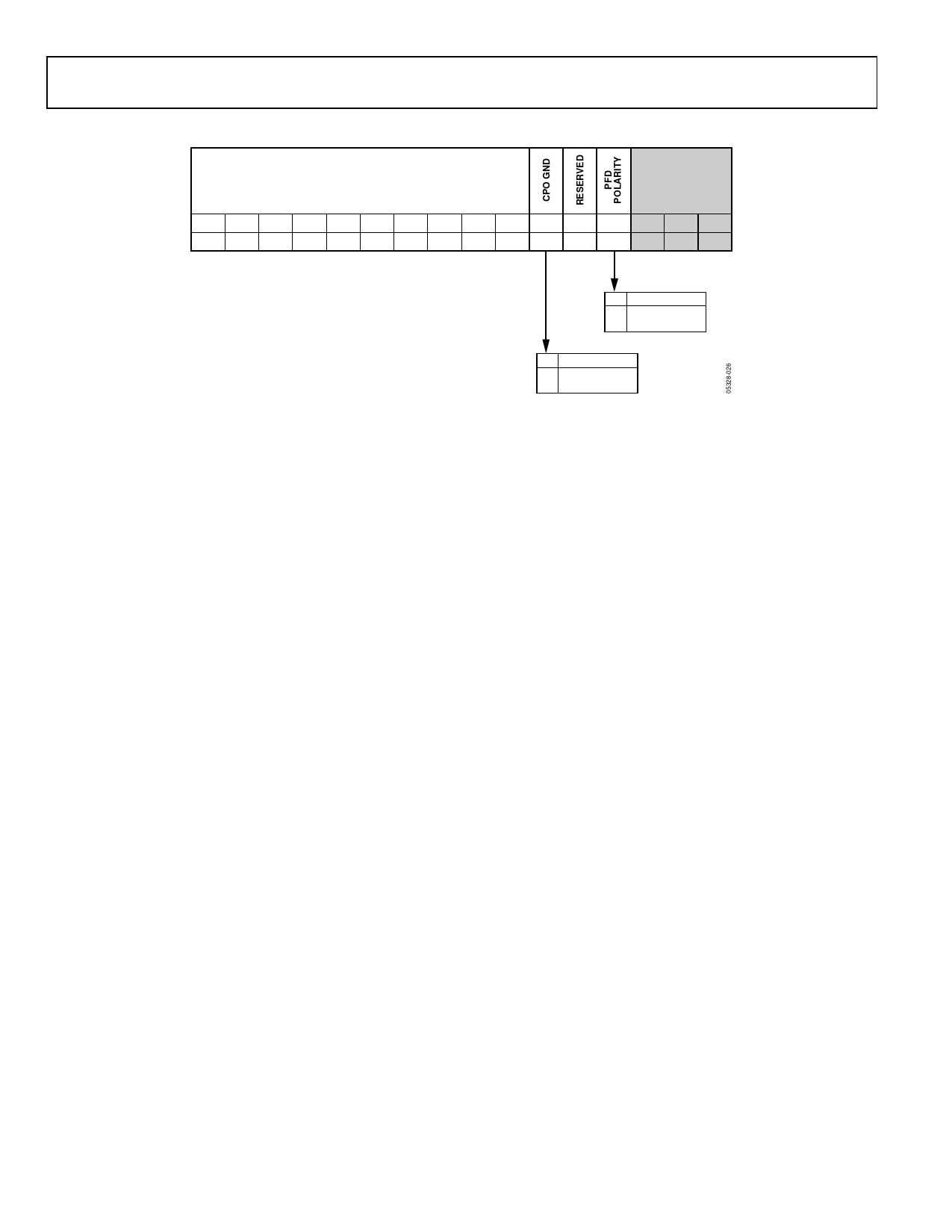
Figure 32. Function Register (R3)
R3, the function register (C3, C2, C1 set to 0, 1, 1, respectively),
only needs to be programmed during the initialization sequence
(see Table 8).
CPO GND
When the CPO GND bit is low, the charge pump outputs
are internally pulled to ground. This is invoked during the
initialization sequence to discharge the loop filter capacitors.
For normal operation, this bit should be high.
PFD Polarity
This bit should be set to 1 for positive polarity and set to 0 for
negative polarity.
Reserved Bits
The Bit DB15 to Bit DB6 are reserved bits and should be
programmed to hex code 001, and Reserved Bit DB4 should be
set to 1.
Rev. F | Page 18 of 32
Share Link: 