ADM488ABRZ Ver la hoja de datos (PDF) - Analog Devices
Número de pieza
componentes Descripción
Lista de partido
ADM488ABRZ Datasheet PDF : 16 Pages
| |||
ADM488A/ADM489A
THEORY OF OPERATION
The ADM488A/ADM489A are ruggedized RS-485 transceivers
that operate from a single 5 V supply. They contain protection
against radiated and conducted interference and are ideally suited
for operation in electrically harsh environments or where cables
can be plugged/unplugged. They are also immune to high RF
field strengths without special shielding precautions.
The ADM488A/ADM489A are intended for balanced data
transmission and comply with both EIA RS-485 and RS-422
standards. They contain a differential line driver and a differen-
tial line receiver, and are suitable for full-duplex data transmission.
The input impedance on the ADM488A/ADM489A is 12 kΩ,
allowing up to 32 transceivers on the differential bus. The
ADM488A/ADM489A operate from a single 5 V ± 10% power
supply. A thermal shutdown circuit prevents excessive power
dissipation caused by bus contention or by output shorting.
This feature forces the driver output into a high impedance state
if, during fault conditions, a significant temperature increase is
detected in the internal driver circuitry.
The receiver contains a fail-safe feature that results in a logic
high output state if the inputs are unconnected (floating).
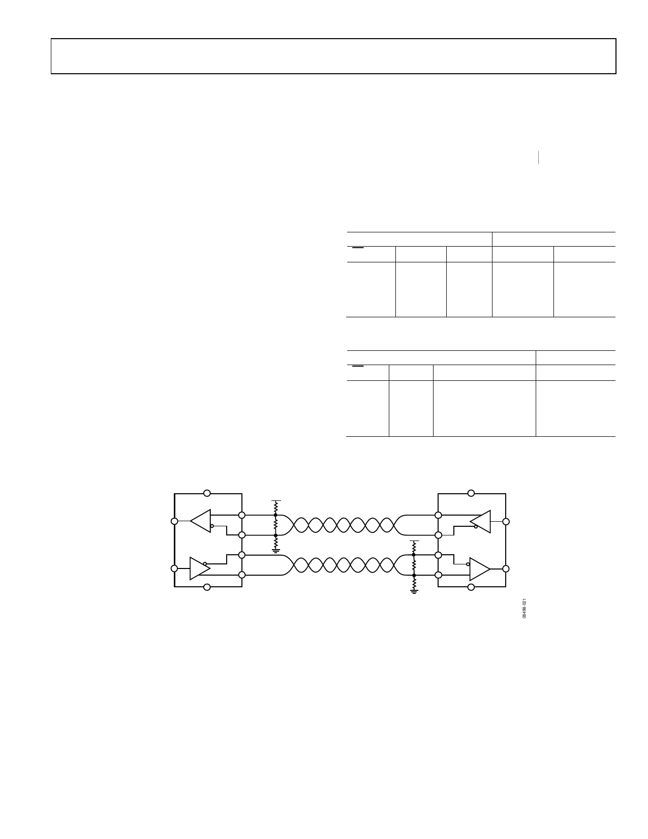
The ADM488A/ADM489A can transmit at data rates up to
250 kbps. Figure 20 shows a typical application for the
ADM488A/ADM489A, a full-duplex link where data transfers
at rates of up to 250 kbps. A terminating resistor is shown at
both ends of the link. This termination is not critical because
the slew rate is controlled by the ADM488A/ADM489A and
reflections are minimized.
The communications network can be extended to include
multipoint connections, as shown in Figure 22. As many as
32 transceivers can be connected to the bus.
Table 6 and Table 7 show the truth tables for transmitting and
receiving.
Table 6. Transmitting Truth Table
Inputs
RE
DE
DI
Z
X1
1
1
0
X1
1
0
1
0
0
X1
High-Z
1
0
X1
Hgh-Z
1 X is don’t care.
Outputs
Y
1
0
High-Z
High-Z
Table 7. Receiving Truth Table
Inputs
RE
DE
A to B
0
0
0
0
≥ +0.2 V
≤ −0.2 V
0
0
1
0
Inputs open circuit
X1
1 X is don’t care.
Output
RO
1
0
1
High-Z
VCC
ADM488A
RO
R
DI
D
VCC
A
B
RT
Z
Y
VCC
ADM488A
Y
Z
VCC
B
D
DI
RT
A
R
RO
GND
GND
NOTES
1. MAXIMUM NUMBER OF NODES = 32.
Figure 20. ADM488A/ADM489A Full-Duplex Data Link
Rev. 0 | Page 11 of 16
Share Link: 