ADM488 Ver la hoja de datos (PDF) - Analog Devices
Número de pieza
componentes Descripción
Lista de partido
ADM488 Datasheet PDF : 16 Pages
| |||
ADM488/ADM489
PIN CONFIGURATIONS AND FUNCTION DESCRIPTIONS
VCC 1
8A
RO 2 ADM488 7 B
TOP VIEW
DI 3 (Not to Scale) 6 Z
GND 4
5Y
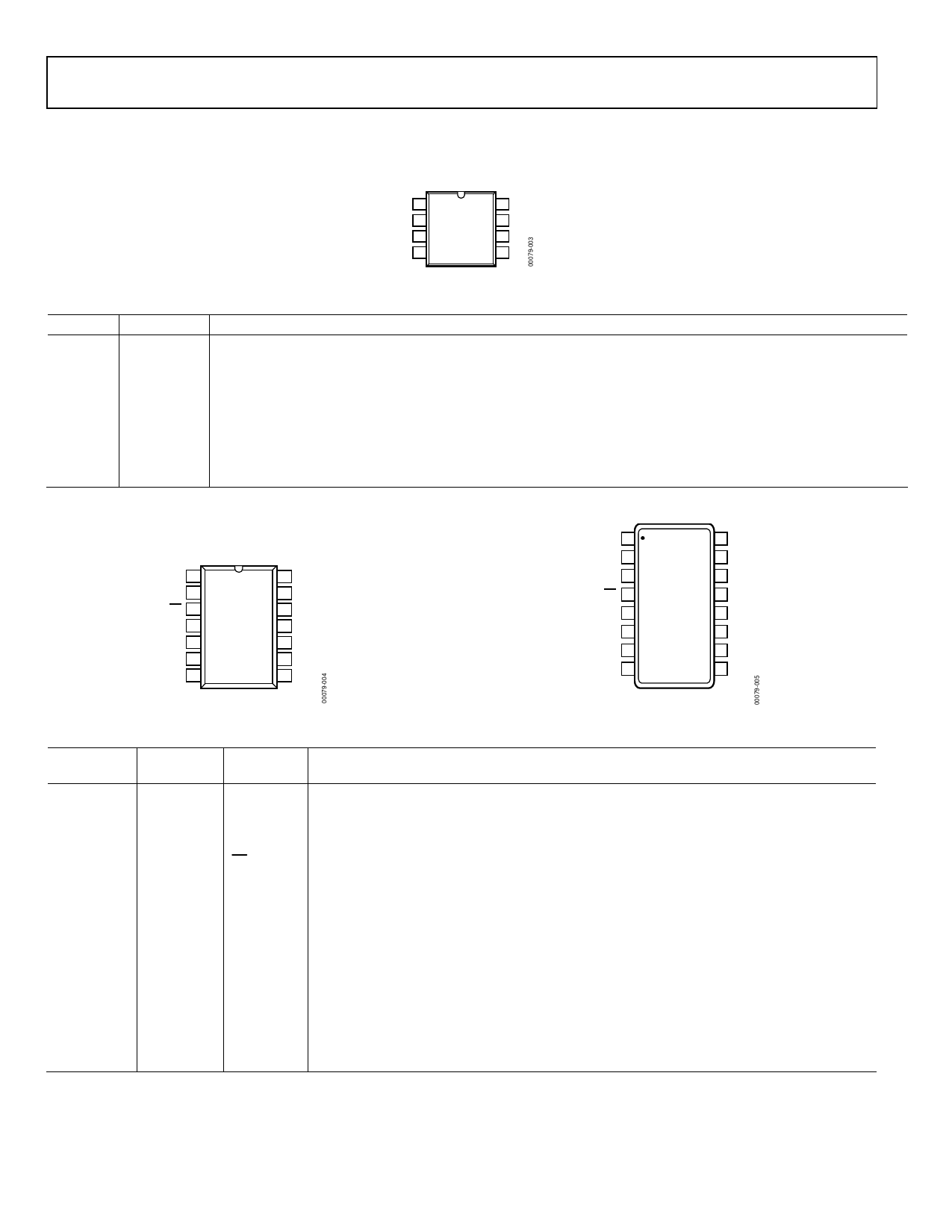
Figure 3. ADM488 8-Lead PDIP/SOIC Pin Configuration
Table 4. ADM488 Pin Function Descriptions
Pin No. Mnemonic Description
1
VCC
Power Supply, 5 V ± 10%.
2
RO
Receiver Output. When A > B by 200 mV, RO = high. If A < B by 200 mV, RO = low.
3
DI
Driver Input. A logic low on DI forces Y low and Z high, while a logic high on DI forces Y high and Z low.
4
GND
Ground Connection, 0 V.
5
Y
Noninverting Driver, Output Y.
6
Z
Inverting Driver, Output Z.
7
B
Inverting Receiver, Input B.
8
A
Noninverting Receiver, Input A.
NC 1
RO 2
RE 3
DE 4
DI 5
GND 6
GND 7
ADM489
TOP VIEW
(Not to Scale)
14 VCC
13 NC
12 A
11 B
10 Z
9Y
8 NC
VCC 1
NC 2
RO 3
RE 4
DE 5
DI 6
GND 7
GND 8
16 NC
15 A
ADM489
TOP VIEW
(Not to Scale)
14 B
13 NC
12 Z
11 Y
10 NC
9 NC
NC = NO CONNECT
NC = NO CONNECT
Figure 4. ADM489 14-Lead PDIP/SOIC Pin Configuration
Figure 5. ADM489 16-Lead TSSOP Pin Configuration
Table 5. ADM489 Pin Function Descriptions
PDIP/SOIC TSSOP
Pin No.
Pin No.
Mnemonic Description
1, 8, 13
2, 9, 10, 13, NC
16
No Connect. No connections are required to this pin.
2
3
RO
Receiver Output. When enabled, if A > B by 200 mV then RO = high. If A < B by 200 mV then
RO = low.
3
4
RE
Receiver Output Enable. A low level enables the receiver output, RO. A high level places it in a
high impedance state.
4
5
DE
Driver Output Enable. A high level enables the driver differential outputs, Y and Z. A low level
places it in a high impedance state.
5
6
DI
Driver Input. When the driver is enabled, a logic low on DI forces Y low and Z high, while a logic
high on DI forces Y high and Z low.
6, 7
7, 8
GND
Ground Connection, 0 V.
9
11
Y
Noninverting Driver, Output Y.
10
12
Z
Inverting Driver, Output Z.
11
14
B
Inverting Receiver, Input B.
12
15
A
Noninverting Receiver, Input A.
14
1
VCC
Power Supply, 5 V ± 10%.
Rev. D | Page 6 of 16
Share Link: 