LT1675CS8-1 Ver la hoja de datos (PDF) - Linear Technology
Número de pieza
componentes Descripción
Lista de partido
LT1675CS8-1 Datasheet PDF : 16 Pages
| |||
LT1675/LT1675-1
APPLICATIONS INFORMATION
Switching Transients
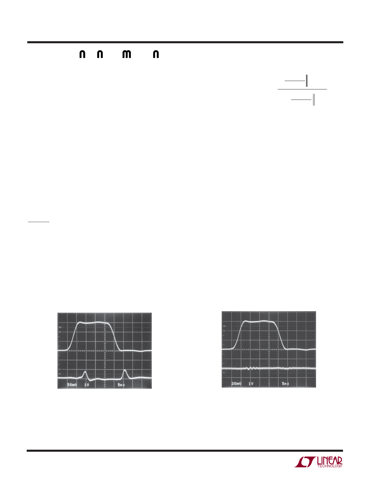
This MUX includes fast current steering break-before-
make SPDT switches that minimize switching glitches.
The switching transients of Figure 3 are input-referred
(measured between 75Ω back termination and the 75Ω
load). The glitch is only 50mVP-P and the duration is just
5ns. This transient is small and fast enough to not be
visible on quality graphics terminals. Additionally, the
break-before-make SPDT switch is open before the alter-
nate channel is connected. This means there is no input
feedthrough during switching. Figure 4 shows the amount
of alternate channel that is coupled at the input.
Expanding Inputs
In video routing applications where the ultimate speed is
not mandatory, as it is in pixel switching, it is possible to
expand the number of MUX inputs by shorting the
LT1675 outputs together and switching with the
ENABLE pins. The internal gain set resistors have a nomi-
nal value of 750Ω and cause a 1500Ω shunt across the
75Ω cable termination. Figure 5 shows schematically the
effect of expanding the number of inputs. The effect of this
loading is to cause a gain error that can be calculated by
the following formula:
Gain
Error
(dB)
=
6dB
+
⎛
20log ⎜⎜
⎜
⎝
751+n517–n5517Ω–51Ω75Ω75Ω⎞⎠⎟⎟⎟
dB
where n is total number of LT1675s. For example, using
ten LT1675s (20 Red, 20 Green and 20 Blue) the Gain Error
is only – 1.7dB per channel.
Figure 6 shows a 4-input RGB router. The response from
RED 1 Input to Red Output is shown in Figure 7 for a
25MHz square wave with Chip Select = 0V. In this case the
Gain Error is – 0.23dB. Toggling with Chip Select between
IC #1 and IC #2 is shown in Figure 8. In this case RED 1
Input is connected to 0V and RED 3 Input is connected to
an uncorrelated sinewave.
3V
SELECT
PIN 10
0V
1V/DIV
RED OUT
PIN 15 0V
50mV/DIV
RL = 150Ω, 10pF SCOPE PROBE
1675 F03
Figure 3. Input-Referred Switching Transient
3V
SELECT
PIN 10
0V
RED 1 IN
PIN 1
0V
1V/DIV
20mV/DIV
RS = 75Ω
1675 F04
Figure 4. Switching Transient at RED 1 (Pin 1)
16751fb
10
Share Link: 