AIC1190-25GT3TB Ver la hoja de datos (PDF) - Analog Intergrations
Número de pieza
componentes Descripción
Lista de partido
AIC1190-25GT3TB Datasheet PDF : 19 Pages
| |||
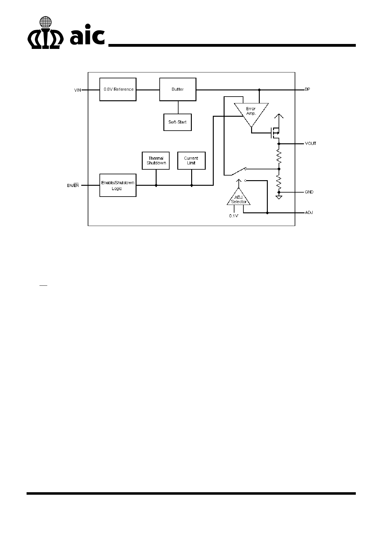
BLOCK DIAGRAM
AIC1190
PIN DESCRIPTION
VIN
– Power supply input pin. Bypass with a 2.2µF capacitor to GND
GND
– Ground.
VOUT
– Regulator Output pin. Sources up to 1A.
EN (5 Pin and 8 Pin) – Chip Enable (Active Low). This pin isn’t allowed to float.
EN (5 Pin and 8 Pin) – Chip Enable (Active High). This pin isn’t allowed to float.
BP (5 Pin and 8 Pin) – Bypass pin. It can connect to external 22nF capacitor to GND to reduce output noise.
The bypass pin could be floating if it’s unnecessary (Keep floating cannot pull low and
pull high).
ADJ (5 Pin and 8 Pin) – The output voltage can either be set by the internal feedback resistors when this pin is
grounded, or be set by the external feedback resistors when using a resistive divider.
11
Share Link: 