AO3435 Ver la hoja de datos (PDF) - Unspecified
Número de pieza
componentes Descripción
Lista de partido
AO3435 Datasheet PDF : 4 Pages
| |||
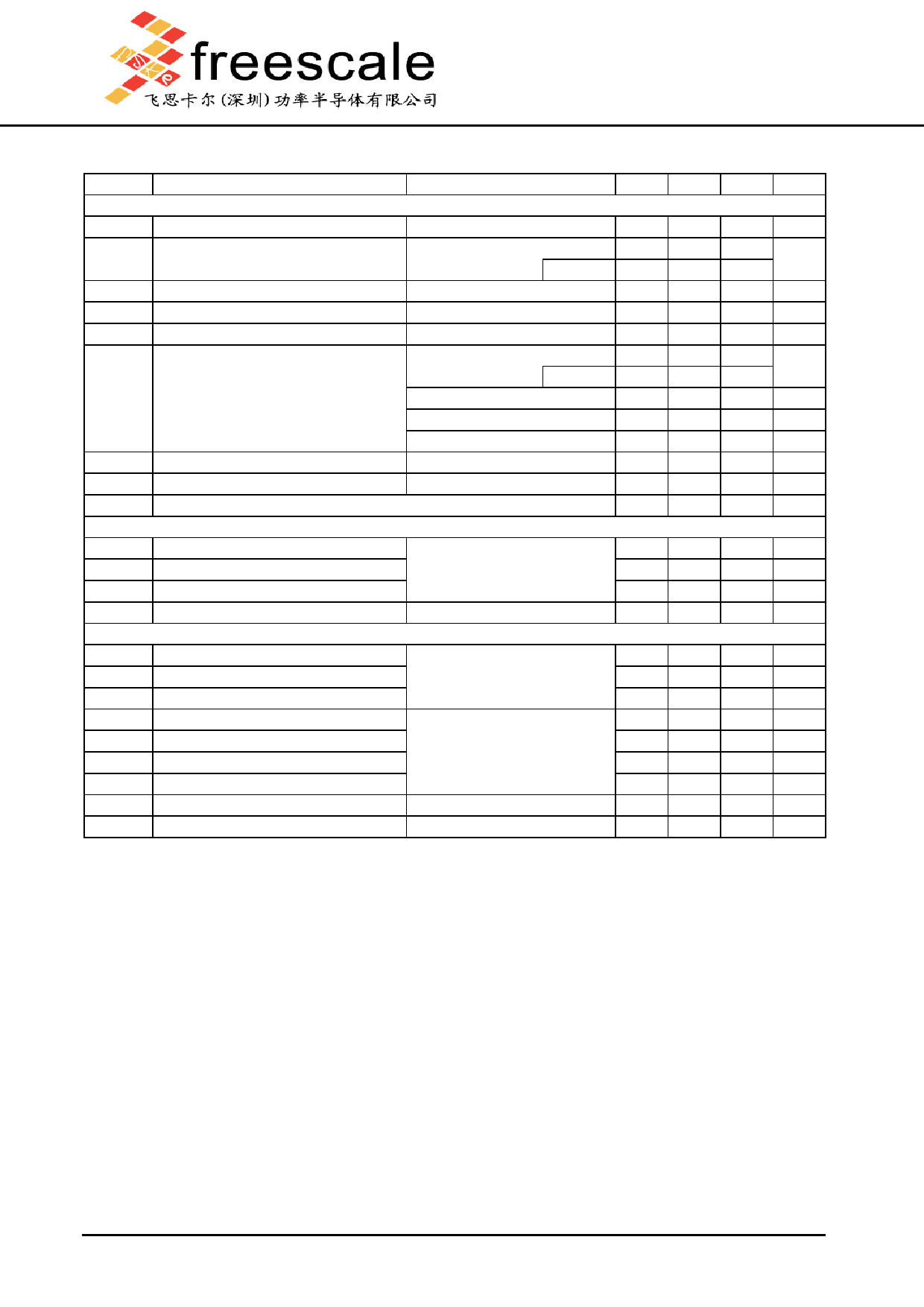
AO3435
20V P-Channel MOSFET
Electrical Characteristics (TJ=25°C unless otherwise noted)
Symbol
Parameter
Conditions
Min Typ Max Units
STATIC PARAMETERS
BVDSS Drain-Source Breakdown Voltage
ID=-250µA, VGS=0V
-20
V
IDSS
Zero Gate Voltage Drain Current
VDS=-20V, VGS=0V
TJ=55°C
-1
µA
-5
IGSS
Gate-Body leakage current
VDS=0V, VGS=±8V
±100 nA
VGS(th) Gate Threshold Voltage
VDS=VGS ID=-250µA
-0.5 -0.65 -1
V
ID(ON)
On state drain current
VGS=-4.5V, VDS=-5V
-25
A
VGS=-4.5V, ID=-3.5A
TJ=125°C
56
70
mΩ
80 100
RDS(ON) Static Drain-Source On-Resistance
VGS=-2.5V, ID=-3.0A
70
90 mΩ
VGS=-1.8V, ID=-2.0A
85 110 mΩ
VGS=-1.5V, ID=-0.5A
100 130 mΩ
gFS
Forward Transconductance
VDS=-5V, ID=-3.5A
15
S
VSD
Diode Forward Voltage
IS=-1A,VGS=0V
-0.7 -1
V
IS
Maximum Body-Diode Continuous Current
-1.4 A
DYNAMIC PARAMETERS
Ciss
Input Capacitance
Coss
Output Capacitance
Crss
Reverse Transfer Capacitance
Rg
Gate resistance
VGS=0V, VDS=-10V, f=1MHz
VGS=0V, VDS=0V, f=1MHz
560 745 pF
80
pF
70
pF
15
23
Ω
SWITCHING PARAMETERS
Qg
Total Gate Charge
8.5 11 nC
Qgs
Gate Source Charge
VGS=-4.5V, VDS=-10V, ID=-3.5A
1.2
nC
Qgd
Gate Drain Charge
2.1
nC
tD(on)
Turn-On DelayTime
7.2
ns
tr
tD(off)
Turn-On Rise Time
Turn-Off DelayTime
VGS=-4.5V, VDS=-10V, RL=3Ω,
36
ns
RGEN=6Ω
53
ns
tf
Turn-Off Fall Time
56
ns
trr
Body Diode Reverse Recovery Time IF=-3.5A, dI/dt=100A/µs
37
49
ns
Qrr
Body Diode Reverse Recovery Charge IF=-3.5A, dI/dt=100A/µs
27
nC
A: The value of R θJA is measured with the device mounted on 1 in 2 FR-4 board with 2oz. copper, in a still air environment with TA=25°C. The
value in any given application depends on the user's specific board design. The current rating is based on the t ≤10s thermal resistance rating.
B: Repetitive rating, pulse width limited by junction temperature.
C. The R θJA is the sum of the thermal impedence from junction to lead R θJL and lead to ambient.
D. The static characteristics in Figures 1 to 6 are obtained using 300µs pulse width, duty cycle 0.5% max.
E. These tests are performed with the device mounted on 1 in 2 FR-4 board with 2oz. Copper, in a stil1l a2ir environment with T A=25°C. The SOA
curve provides a single pulse rating.
Rev1 : Nov. 2010
THIS PRODUCT HAS BEEN DESIGNED AND QUALIFIED FOR THE CONSUMER MARKET. APPLICATIONS OR USES AS CRITICAL
COMPONENTS IN LIFE SUPPORT DEVICES OR SYSTEMS ARE NOT AUTHORIZED. AOS DOES NOT ASSUME ANY LIABILITY ARISING
OUT OF SUCH APPLICATIONS OR USES OF ITS PRODUCTS. AOS RESERVES THE RIGHT TO IMPROVE PRODUCT DESIGN,
FUNCTIONS AND RELIABILITY WITHOUT NOTICE.
2/4
www.freescale.net.cn
Share Link: 