AP1084T25LA Ver la hoja de datos (PDF) - Anachip Corporation
Número de pieza
componentes Descripción
Lista de partido
AP1084T25LA Datasheet PDF : 11 Pages
| |||
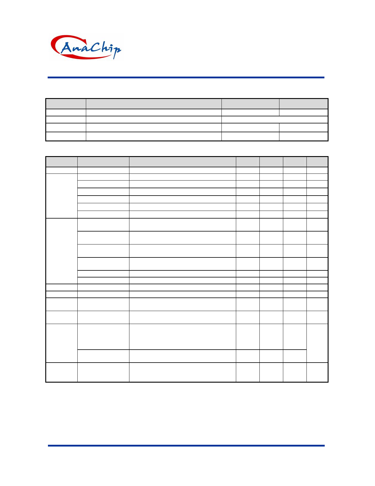
AP1084
5A Low Dropout Positive Adjustable or Fixed-Mode Regulator
Absolute Maximum Ratings
Symbol
Vin
PD
TST
TOP
Parameter
DC Supply Voltage
Power Dissipation
Storage Temperature
Operating Junction Temperature Range
Rating
Unit
-0.3 to 12
V
Internally Limited
-65 to +150
oC
0 to +150
oC
Electrical Characteristics (Under Operating Conditions)
Sym.
Parameter
Conditions (Notes)
VREF
Reference Voltage
AP1084-XXX
AP1084-1.5
Line AP1084-1.8
Regulation AP1084-2.5
AP1084-3.3
AP1084-5.0
AP1084-Adj
AP1084-1.5
Io=10mA, Tj=25oC, (Vin-Vout)=1.5V
IO=10mA, VOUT+1.5V<VIN<12V, TJ =25oC
IOUT = 10mA, TJ = 25oC, 3V≦VIN≦12V
IOUT = 10mA, TJ = 25oC, 3.3V≦VIN≦12V
IOUT = 10mA, TJ = 25oC, 4V≦VIN≦12V
IOUT = 10mA, TJ = 25oC, 4.8V≦VIN≦12V
IOUT = 10mA, TJ = 25oC, 6.5V≦VIN≦12V
VIN=3.3V, 0mA<Io<5A, TJ =25oC
(Note 1,2)
VIN=3V, 0mA<Io<5A, TJ =25oC
(Note 1,2)
Load
Regulation
AP1084-1.8
AP1084-2.5
AP1084-3.3
AP1084-5.0
∆Vo Dropout Voltage
VIN=3.3V, 0mA<Io<5A
TJ =25oC (Note 1,2)
VIN=4V, 0mA<Io<5A
TJ =25oC (Note 1,2)
VIN = 5V, 0mA<Io<5A , TJ=25oC (Note 1,2)
VIN = 8V, 0mA<Io<5A, TJ=25oC (Note 1,2)
Io=5.0A (∆Vout = 1% Vout)
Current Limit
Vin-Vout=5V
Minimum Load
Current
Temperature
Stability
Io=10mA
θJA
Thermal Resistance
Junction-to-Ambient
(No heat sink ;No
air flow)
TO-252
TO-263
TO-220
Thermal Resistance PDIP-8: Control Circuitry/Power Transistor
Junction-to-Ambient (Note 3)
θJC
Thermal Resistance
Junction-to-Case
TO-252: Control Circuitry/Power Transistor
TO-263: Control Circuitry/Power Transistor
TO-220: Control Circuitry/Power Transistor
Min.
1.225
1.470
1.764
2.450
3.235
4.900
5.1
Typ.
1.250
1.500
1.800
2.500
3.300
5.000
12
15
20
26
40
1.3
5
0.5
98
83
83
35
10
0.65/2.7
0.65/2.7
Max.
1.275
0.2
1.530
1.836
2.550
3.365
5.100
1
15
18
25
33
50
1.4
10
Unit
V
%
V
V
V
V
V
%
mV
mV
mV
mV
mV
V
A
mA
%
OC/W
OC/W
Note 1: See thermal regulation specifications for changes in output voltage due to heating effects. Line and load regulation are measured
at a constant junction temperature by low duty cycle pulse testing. Load regulation is measured at the output lead = 1/18” from the
package.
Note 2: Line and load regulation are guaranteed up to the maximum power dissipation of 15W. Power dissipation is determined by the
difference between input and output and the output current. Guaranteed maximum power dissipation will not be available over the
full input/output range.
Note 3: Output is connected to the PCB cupper area 5.5mm*5.5mm separately. If you need large PD or lower Tc & Tj, please connect to
the large cupper area >> 5.5mm*5.5mm (like 10mm*10mm).
Anachip Corp.
www.anachip.com.tw
Rev.1.2 Jun.9, 2005
3/11
Share Link: 