AP1086 Ver la hoja de datos (PDF) - Diodes Incorporated.
Número de pieza
componentes Descripción
Lista de partido
AP1086 Datasheet PDF : 8 Pages
| |||
AP1086
1.5A LOW DROPOUT POSITIVE ADJUSTABLE OR
FIXED-MODE REGULATOR
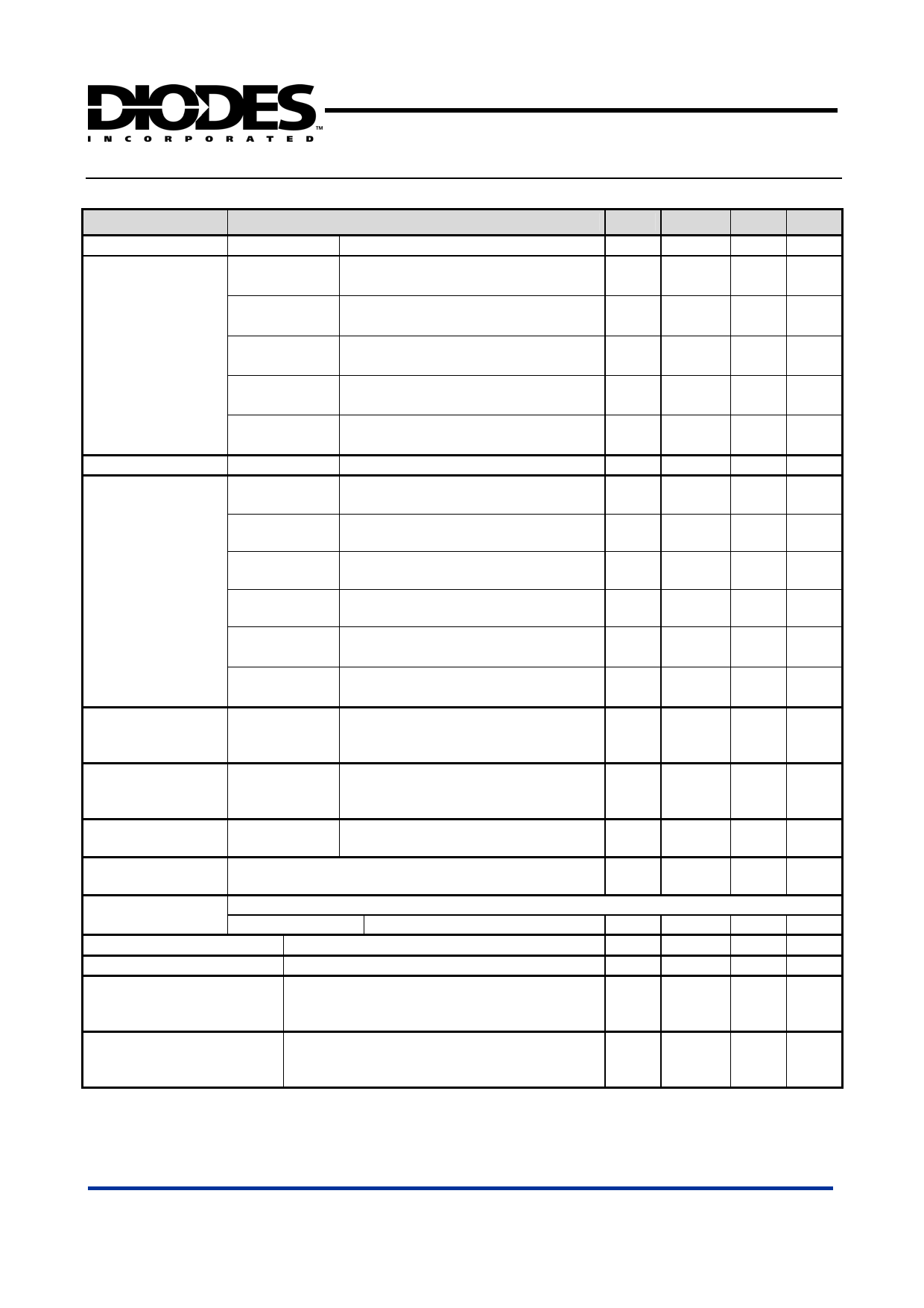
Electrical Characteristics ( Under Operating Conditions )
PARAMETER
CONDITIONS
MIN TYP MAX UNIT
Reference Voltage AP1086-Adj TA = 25οC,(VIN-VOUT)= 1.5V,IO = 10mA 1.225 1.250 1.275 V
AP1086-1.5
IOUT = 10mA, TA = 25οC, 3V≦VIN≦
1.470 1.500 1.530
V
12V
AP1086-1.8
IOUT = 10mA, TA = 25οC, 3.3V≦VIN≦ 1.764 1.800 1.836
V
12V
Output Voltage
AP1086-2.5
IOUT = 10mA, TA = 25οC, 4V≦VIN≦
2.450 2.500 2.550
V
12V
AP1086-3.3
IOUT = 10mA, TA = 25οC, 4.8V≦VIN≦ 3.235 3.300 3.365
V
12V
AP1086-5.0
IOUT = 10mA, TA = 25οC, 6.5V≦VIN≦ 4.900 5.000 5.100
V
12V
Line Regulation AP1086-XXX IO = 10mA, VOUT+1.5V<VIN<12V
-
AP1086-Adj
VIN = 3.3V, 0mA<Io<1.5A, TA = 25οC
(Note 3, 4)
-
AP1086-1.5
VIN = 3V, 0mA<Io<1.5A, TA = 25οC
(Note 3, 4)
-
Load Regulation
AP1086-1.8
AP1086-2.5
VIN = 3.3V, 0mA<Io<1.5A, TA = 25οC
(Note 3, 4)
VIN = 4V, 0mA<Io<1.5A, TA = 25οC
(Note 3, 4)
-
-
AP1086-3.3
VIN = 5V, 0≦IOUT≦1.5A, TA = 25οC ,
TJ = 25oC (Note 3, 4)
-
AP1086-5.0
VIN = 8V, 0≦IOUT≦1.5A, TA = 25οC ,
TJ = 25oC (Note 3, 4)
-
Dropout Voltage
(VIN-VOUT)
AP1086-Adj/-
2.5
IOUT = 1.5A, ∆VOUT = 1%VOUT
/-3.3/-3.6/-5.0
-
-
0.2 %
-
1
%
12
15 mV
15
18 mV
20
25 mV
26
33 mV
40
50 mV
1.3
1.4
V
Current Limit
AP1086-Adj/-
2.5
(VIN-VOUT) = 5V
/-3.3/-3.6/-5.0
1. 6
-
-
A
Minimum Load
Current
AP1086-XXX 0oC≦Tj≦125oC
-
5
10 mA
Thermal
Regulation
TA = 25οC, 30ms pulse
-
0.008 0.04 %/W
Ripple Rejection
f = 120Hz,COUT = 25uF Tantalum, IOUT = 1.5A
AP1086-XXX
VIN = VOUT+3V
RMS Noise (% of VOUT)
10Hz ≤ f ≤ 10KHz
Temperature Stability
IO = 10mA
Thermal Resistance
TO252-3L
Junction-to-Ambient
TO263-3L
(No heat sink ;No air flow) TO220-3L
-
60
70 dB
-
0.003
-
%
-
0.5
-
%
101
-
83
- OC/W
86
Thermal Resistance
Junction-to-Case
TO252-3L: Control Circuitry/Power Transistor
15
TO263-3L: Control Circuitry/Power Transistor - 0.65/2.7 - OC/W
TO220-3L: Control Circuitry/Power Transistor
0.65/2.7
Notes: 3. See thermal regulation specifications for changes in output voltage due to heating effects. Line and load regulation are measured at a
constant junction temperature by low duty cycle pulse testing. Load regulation is measured at the output lead = 1/18” from the package.
4. Line and load regulation are guaranteed up to the maximum power dissipation of 15W. Power dissipation is determined by the difference in input
and output and the output current. Guaranteed maximum power dissipation will not be available over the full input/output range.
5. Quiescent current is defined as the minimum output current required in maintaining regulation. At 12V input/output differential the
device is guaranteed to regulate if the output current is greater than 10mA.
AP1086 Rev. 2
3 of 8
www.diodes.com
MARCH 2007
© Diodes Incorporated
Share Link: 