AS7C33128FT32B Ver la hoja de datos (PDF) - Alliance Semiconductor
Número de pieza
componentes Descripción
Lista de partido
AS7C33128FT32B Datasheet PDF : 19 Pages
| |||
AS7C33128PFS32B
AS7C33128PFS36B
®
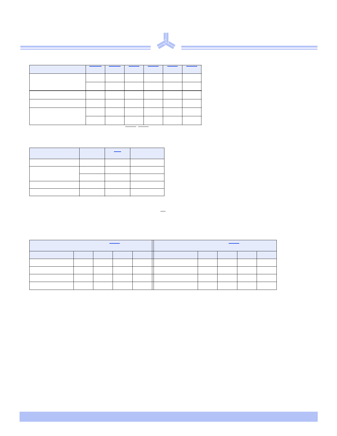
Write enable truth table (per byte)
Function
GWE BWE BWa BWb BWc BWd
Write All Bytes
L
X
X
X
X
X
H
L
L
L
L
L
Write Byte a
H
L
L
H
H
H
Write Byte c and d
H
L
H
H
L
L
H
H
X
X
X
X
Read
H
L
H
H
H
H
Key: X = don’t care, L = low, H = high, n = a, b, c, d; BWE, BWn = internal write signal.
Asynchronous Truth Table
Operation
Snooze mode
Read
Write
Deselected
ZZ
OE
I/O Status
H
X
High-Z
L
L
Dout
L
H
High-Z
L
X
Din, High-Z
L
X
High-Z
Notes:
1. X means “Don’t Care”
2. ZZ pin is pulled down internally
3. For write cycles that follows read cycles, the output buffers must be disabled with OE, otherwise data bus contention will occur.
4. Snooze mode means power down state of which stand-by current does not depend on cycle times
5. Deselected means power down state of which stand-by current depends on cycle times
Burst sequence table
Interleaved burst address (LBO = 1)
A1 A0 A1 A0 A1 A0
1st Address
00
01
10
2nd Address
01
00
11
3rd Address
10
11
00
4th Address
11
10
01
A1 A0
11
10
01
00
Linear burst address (LBO = 0)
A1 A0 A1 A0 A1 A0
1st Address
00
01
10
2nd Address
01
10
11
3rd Address
10
11
00
4th Address
11
10
01
A1 A0
11
00
01
10
12/10/04; v.1.7
Alliance Semiconductor
P. 6 of 19
Share Link: 