IR2131SPBF Ver la hoja de datos (PDF) - International Rectifier
Número de pieza
componentes Descripción
Lista de partido
IR2131SPBF Datasheet PDF : 10 Pages
| |||
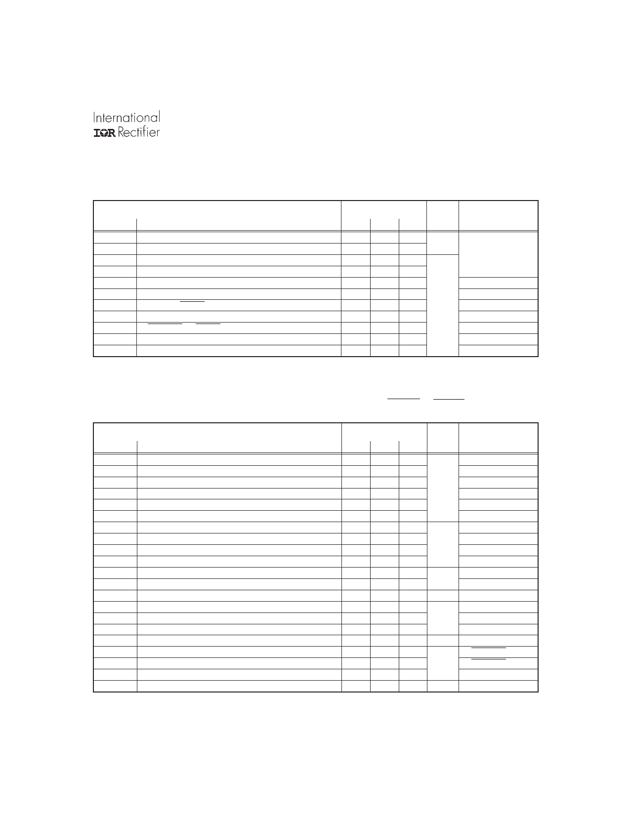
IR2131(J)(S) & (PbF)
Dynamic Electrical Characteristics
VBIAS (VCC, VBS1,2,3) = 15V, VS1,2,3 = VSS = COM, CL = 1000 pF and TA = 25°C unless otherwise specified. The dynamic
electrical characteristics are defined in Figures 4 through 5.
Parameter
Value
Symbol
Definition
Min. Typ. Max. Units Test Conditions
ton
Turn-On Propagation Delay
toff
Turn-Off Propagation Delay
tr
Turn-On Rise Time
tf
Turn-Off Fall Time
titrip
ITRIP to Output Shutdown Propagation Delay
tbl
ITRIP Blanking Time
tflt
ITRIP to FAULT Indication Delay
tflt,in
Input Filter Time (All Six Inputs)
tfltclr
FLT - CLR to FAULT Clear Time
tsd
SD to Output Shutdown Propagation Delay
DT
Deadtime
NOTE: For high side PWM, HIN pulse width must be ≥ 1.5µsec
0.6
1.3 2.0
µs
0.2 0.6 1.0
VIN = 0 & 5V
—
80 150
VS1,2,3 = 0 to 600V
—
40 100
400 700 1000
VIN, VITRIP = 0 & 5V
— 400 —
VITRIP = 1V
400 700 1000 ns VIN, VITRIP = 0 & 5V
— 310 —
VIN = 0 & 5V
400 800 1200
VIN, VIT, VFC = 0&5V
400 700 1000
VIN, VSD = 0 & 5V
400 700 1200
VIN = 0 & 5V
Static Electrical Characteristics
VBIAS (VCC, VBS1,2,3) = 15V, VS1,2,3 = VSS = COM and TA = 25°C unless otherwise specified. The VIN, VTH and IIN
parameters are referenced to VSS and are applicable to all six logic input leads: HIN1,2,3 & LIN1,2,3 . The VO and IO
parameters are referenced to COM and VS1,2,3 and are applicable to the respective output leads: HO1,2,3 or LO1,2,3.
Symbol
VIH
VIL
VFCLR,IH
VFCLR,IL
VSD,TH+
VSD,TH-
VIT,TH+
VIT,TH-
VOH
VOL
ILK
IQBS
IQCC
IIN+
IIN-
IITRIP+
IITRIP-
IFCLR+
IFCLR-
ISD+
ISD-
Parameter
Definition
Logic “0” Input Voltage (OUT = LO)
Logic “1” Input Voltage (OUT = HI)
Logic “0” Fault Clear Input Voltage
Logic “1” Fault Clear Input Voltage
Shutdown Input Positive Going Threshold
Shutdown Input Negative Going Threshold
ITRIP Input Positive Going Threshold
ITRIP Input Negative Going Threshold
High Level Output Voltage, VBIAS - VO
Low Level Output Voltage, VO
Offset Supply Leakage Current
Quiescent VBS Supply Current
Quiescent VCC Supply Current
Logic “1” Input Bias Current (OUT = HI)
Logic “0” Input Bias Current (OUT = LO)
“High” ITRIP Bias Current
“Low” ITRIP Bias Current
Logic “1” Fault Clear Bias Current
Logic “0” Fault Clear Bias Current
Logic “1” Shutdown Bias Current
Logic “0” Shutdown Bias Current
Min.
2.2
—
2.2
—
1.2
0.9
250
200
—
—
—
—
—
—
—
—
—
—
—
—
—
Value
Typ. Max. Units
——
— 0.8
—
—
V
— 0.8
1.8 2.1
1.5 1.8
485 600
400 550 mV
— 100
— 100
—
50
µA
30 100
3.0 4.5 mA
190 300
50 100 µA
75 150
— 100 nA
125 250
75 150 µA
75 150
— 100 nA
Test Conditions
VIN = 0V, IO = 0A
VIN = 5V, IO = 0A
VB = VS = 600V
VIN = 0V or 5V
VIN = 0V or 5V
VIN = 0V
VIN = 5V
ITRIP = 5V
ITRIP = 0V
FLT - CLR = 0V
FLT - CLR = 5V
SD = 5V
SD = 0V
www.irf.com
3
Share Link: 