AV9170 Ver la hoja de datos (PDF) - Integrated Circuit Systems
Número de pieza
componentes Descripción
Lista de partido
AV9170 Datasheet PDF : 11 Pages
| |||
AV9170
Using the AV9170
The AV9170 has the following characteristics:
1. Rising edges at IN and FBIN are lined up. Falling
edges are not synchronized.
2. The relationship between the frequencies at FBIN and IN
with CLK1 feedback is shown in Table 1 below.
Functionality (Table 1:)
FS1 FS0 fFBIN (-01, -02) fFBIN (-04, -05)
0
0
2 • fIN
3 • fIN
0
1
4 • fIN
5 • fIN
1
0
fIN
6 • fIN
1
1
8 • fIN
10 • fIN
3. The frequency of CLK2 is half the CLK1 frequency.
4. The CLK1 frequency ranges are:
VDD = 5V VDD = 3.3V
AV9170-01, -04 20 < fCLK1 < 107 MHz* < 66.7
AV9170-02, -05 5 < fCLK1 < 26.75 MHz* < 16.7
The AV9170 will only operate correctly within these
frequency ranges.
Eliminate High Speed
Clock Routing Problems
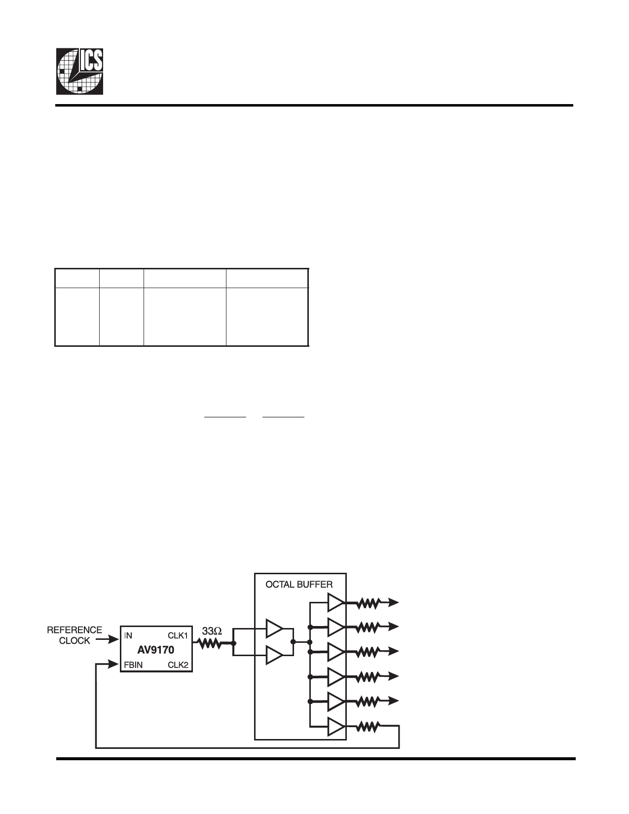
The AV9170 makes it possible to route lower speed clocks
over long distances on the PC board and to place an AV9170
next to the device requiring a higher speed clock. The
multiplied output can then be used to produce a phase locked,
higher speed output clock.
Compensate for Propagation Delays
Including an AV9170 in a timing loop allows the use of PALs,
gate arrays, etc., with loose timing specifications. The
AV9170 compensates for the delay through the PAL and
synchronizes the output to the input reference clock.
Operating Frequency Range
The AV9170 is offered in versions optimized for operation
in two frequency ranges. The -01 and -04 cover high
frequencies, 20 to 100 MHz.* The -02 and -05 operate from
5 to 25 MHz.* The AV9170 can be supplied with custom
multiplication factors and operating ranges. Consult ICS for
details.
3.3V VDD Operation
The AV9170 does operate at both 5.0V and 3.3V system
conditions. Please note the Electrical Characteristic specifica-
tions at 3.3V include a limited output frequency (66.6 MHz
max.) and a wider skew of FBIN to CLK1. For 3.3V±5%
(3.15V min.), this skew is -5.0 to 0 ns. At 3.3V±10% (3.0V
min.), the skew is widened to -8 ns to 0 ns and should be
accounted for in system design.
Figure 1:
Application of
AV9170 for Multiple Outputs
*At 3.3V, the maximum CLK1 frequency is 66.7 MHz for -01,
-04 and 16.7 MHz for -02, -05.
3
Share Link: 