BS616LV2019AC Ver la hoja de datos (PDF) - Brilliance Semiconductor
Número de pieza
componentes Descripción
Lista de partido
BS616LV2019AC Datasheet PDF : 10 Pages
| |||
BSI
BS616LV2019
AC ELECTRICAL CHARACTERISTICS ( TA = -40 to + 85oC )
WRITE CYCLE (48B BGA ignore CE2 condition)
JEDEC
PARAMETER
NAME
tAVAX
tE1LWH
t
AVWL
tAVWH
t
WLWH
tWHAX
tBW
t
WLQZ
tDVWH
tWHDX
tGHQZ
tWHOX
PARAMETER
NAME
tWC
tCW
tAS
tAW
tWP
tWR
t (1)
BW
tWHZ
tDW
tDH
tOHZ
tOW
DESCRIPTION
Write Cycle Time
Chip Select to End of Write
Address Setup Time
(CE,CE2)
Address Valid to End of Write
Write Pulse Width
Write recovery Time
(CE,CE2,WE)
Date Byte Control to End of Write
(LB,UB)
Write to Output in High Z
Data to Write Time Overlap
Data Hold from Write Time
Output Disable to Output in High Z
End of Write to Output Active
CYCLE TIME : 55ns
(Vcc = 2.7~3.6V)
MIN. TYP. MAX.
55 --
--
55 --
--
0
--
--
55 --
--
30 --
--
0
--
--
25 --
--
-- -- 25
25 --
--
0
--
--
-- -- 25
5
--
--
CYCLE TIME : 70ns
(Vcc = 2.7~3.6V)
MIN. TYP. MAX.
70 --
--
70 --
--
0
--
--
70 --
--
35 --
--
0
--
--
30 --
--
--
--
30
30 --
--
0
--
--
--
--
30
5
--
--
UNIT
ns
ns
ns
ns
ns
ns
ns
ns
ns
ns
ns
ns
NOTE :
1. tBW is 25ns/30ns (@speed=55ns/70ns) with address toggle. ; tBW is 55ns/70ns (@speed=55ns/70ns) without address toggle.
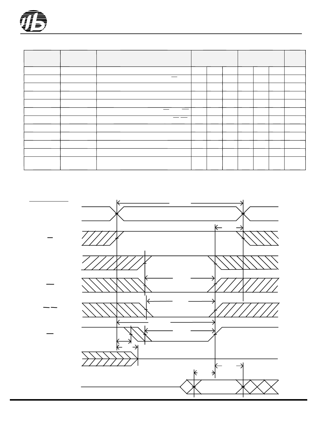
SWITCHING WAVEFORMS (WRITE CYCLE)
WRITE CYCLE1 (1)
t WC
ADDRESS
(3)
t WR
OE
CE2
CE
LB,UB
WE
D OUT
D IN
R0201-BS616LV2019
t AS
(4,10)
t OHZ
(5,12)
(5)
(11)
t CW
(5)
t AW
t BW
t WP
(2)
t DW
(3)
t DH
6
Revision 1.2
May 2004
Share Link: 