US1050-33 Ver la hoja de datos (PDF) - Unisem
Número de pieza
componentes Descripción
Lista de partido
US1050-33 Datasheet PDF : 3 Pages
| |||
US1050-33
PIN DESCRIPTIONS
PIN #
1
2
3
PIN SYMBOL
Gnd
Vout
Vin
PIN DESCRIPTION
This pin must be connected to GND plane using a low inductance short connection.
The output of the regulator. A minimum of 10uF capacitor must be connected
from this pin to ground to insure stability.
The input pin of the regulator. Typically a large storage capacitor is connected
from this pin to ground to insure that the input voltage does not sag below the
minimum drop out voltage during the load transient response. This pin must
always be 1.3V higher than Vout in order for the device to regulate properly.
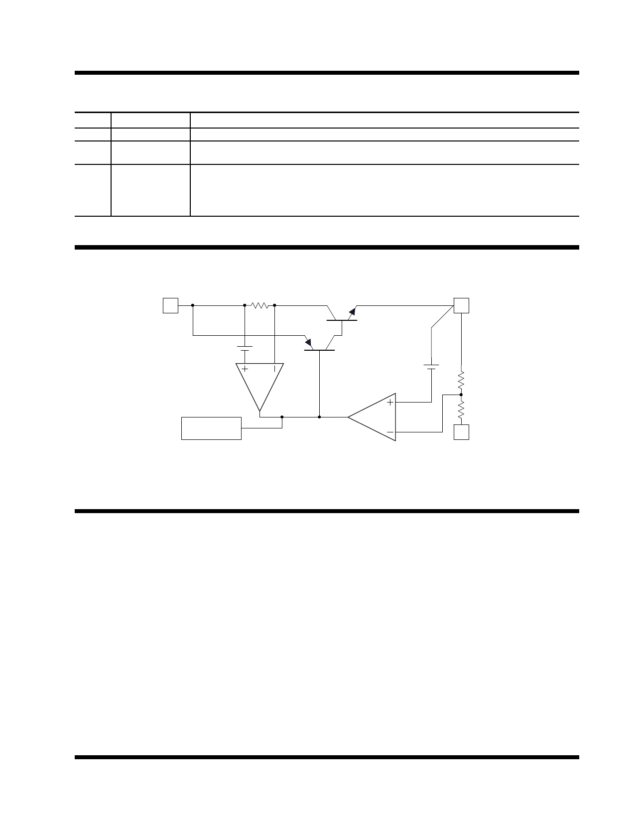
BLOCK DIAGRAM
Vin 3
2 Vout
+
CURRENT
LIMIT
THERMAL
SHUTDOWN
1.25V +
1050-33blk1-1.0
1 Gnd
Figure 1 - Simplified block diagram of the US1050-33
APPLICATION INFORMATION
Stability
The US1050-33 requires the use of an output capacitor
as part of the frequency compensation in order to make
the regulator stable. Typical designs for microproces-
sor applications use standard electrolytic capacitors with
a typical ESR in the range of 50 to 100 mΩ and an
output capacitance of 500 to 1000uF. Fortunately as
the capacitance increases, the ESR decreases result-
ing in a fixed RC time constant. The US1050-33 takes
advantage of this phenomena in making the overall regu-
lator loop stable.For most applications a minimum of
100uF aluminum electrolytic capacitor such as Sanyo
MVGX series ,Panasonic FA series as well as the
Nichicon PL series insures both stability and good tran-
sient response.
Rev. 1.1
10/27/00
2-35
Share Link: 