PI6C39911 Ver la hoja de datos (PDF) - Pericom Semiconductor Corporation
Número de pieza
componentes Descripción
Lista de partido
PI6C39911
Pericom Semiconductor Corporation

PI6C39911 Datasheet PDF : 11 Pages
| |||
PI6C39911/PI6C39912
3.3V High Speed LVTTL or Balanced Output
11223344556677889900112233445566778899001122334455667788990011221122334455667788990011223344556677889900112233445566778899001122112233445566778899001122P3344r5566o77g8899r00a1122m3344m556677a88b9900l11e2211S2233k44e5566w7788C990011l22o33c44k556677B8899u0011f22f33e44r5566-7788S99u0011p2211e22r33C4455l66o7788c99k0011®22
Figure 3 shows a configuration to equalize skew between metal
traces of different lengths. In addition to low skew between outputs,
the SuperClock can be programmed to stagger the timing of its
outputs. The four groups of output pairs can each be programmed
to different output timing. Skew timing can be adjusted over a wide
range in small increments with the appropriate strapping of the
function select pins. In this configuration the 4Q0 output is fed back
to FB and configured for zero skew.
The other three pairs of outputs are programmed to yield different
skews relative to the feedback. By advancing the clock signal on the
longer traces or retarding the clock signal on shorter traces, all loads
can receive the clock pulse at the same time.
In this illustration the FB input is connected to an output with 0ns
skew (xF1, xF0 = MID) selected. The internal PLL synchronizes the
FB and REF inputs and aligns their rising edges to insure that all
outputs have precise phase alignment.
Clock skews can be advanced by ±6 time units (tU) when using an
output selected for zero skew as the feedback. A wider range of
delays is possible if the output connected to FB is also skewed. Since
Zero Skew, +tU, and tU are defined relative to output groups, and
since the PLL aligns the rising edges of REF and FB, it is possible to
create wider output skews by proper selection of the xFn inputs. For
example a +10 tU between REF and 3Qx can be achieved by connect-
ing 1Q0 to FB and setting 1F0 = 1F1 = GND, 3F0 = MID, and 3F1 =
High. (Since FB aligns at 4 tU and 3Qx skews to +6 tU , a total of +10
tU skew is realized). Many other configurations can be realized by
skewing both the output used as the FB input and skewing the other
outputs.
REF
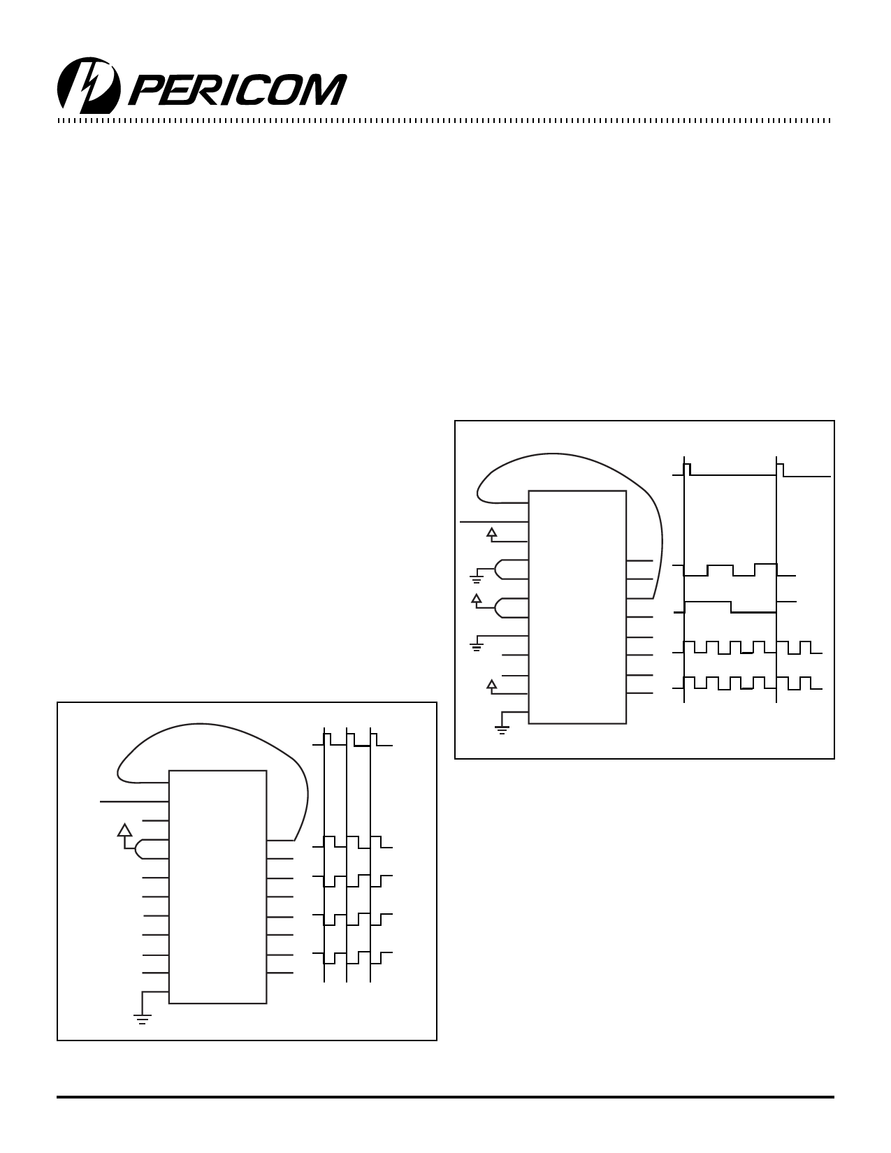
Figure 4 shows an example of the invert function of the SuperClock.
In this example the 4Q0 output used as the FB input is programmed
for invert (4F0 = 4F1 = HIGH) while the other three pairs of outputs
are programmed for zero skew. When 4F0 and 4F1 are tied HIGH, 4Q0
and 4Q1 become inverted zero phase outputs. The PLL aligns the
rising edge of the FB input with the rising edge of the REF. This
causes the 1Q, 2Q, and 3Q outputs to become the inverted outputs
with respect to the REF input. By selecting which output is connect
to FB, it is possible to have 2 inverted and 6 non-inverted outputs
or 6 inverted and 2 non-inverted outputs. The correct configuration
would be determined by the need for more (or fewer) inverted
outputs. 1Q, 2Q, and 3Q outputs can also be skewed to compensate
for varying trace delays independent of inver-sion on 4Q.
20 MHz
FB
REF
FS
4F0
4F1
3F0
3F1
2F0
2F1
1F0
1F1
TEST
REF
4Q0
4Q1
3Q0
3Q1
2Q0
2Q1
1Q0
1Q1
40 MHz
20 MHz
80 MHz
FB
REF
FS
4F0
4Q0
4F1
4Q1
3F0
3Q0
3F1
3Q1
2F0
2Q0
2F1
2Q1
1F0
1Q0
1F1
1Q1
TEST
Figure 4. Inverted Output Connections
Figure 5. Frequency Multiplier with Skew Connections
Figure 5 illustrates the SuperClock configured as a clock multiplier.
The 3Q0 output is programmed to divide by four and is fed back to
FB. This causes the PLL to increase its frequency until the 3Q0 and
3Q1 outputs are locked at 20 MHz while the 1Qx and 2Qx outputs run
at 80 MHz. The 4Q0 and 4Q1 outputs are programmed to divide by
two, which results in a 40 MHz waveform at these outputs. Note that
the 20 and 40 MHz clocks fall simultaneously and are out of phase
on their rising edge. This will allow the designer to use the rising
edges of the ½ frequency and ¼ frequency outputs without concern
for rising-edge skew. The 2Q0, 2Q1, 1Q0, and 1Q1 outputs run at 80
MHz and are skewed by programming their select inputs accord-
ingly. Note that the FS pin is wired for 80 MHz operation because that
is the frequency of the fastest output.
8
PS8497A 04/10/01
Share Link: