PI6C2305-1LI Ver la hoja de datos (PDF) - Pericom Semiconductor
Número de pieza
componentes Descripción
Lista de partido
PI6C2305-1LI Datasheet PDF : 9 Pages
| |||
PI6C2305/PI6C2309
Zero Delay Clock Buffer 1122334455667788990011223344556677889900112233445566778899001122112233445566778899001122334455667788990011223344556677889900112211223344556677889900112233445566778899001122334455667788990011221122334455667788990011223344556677889900112233445566778899001122112233445566778899001122
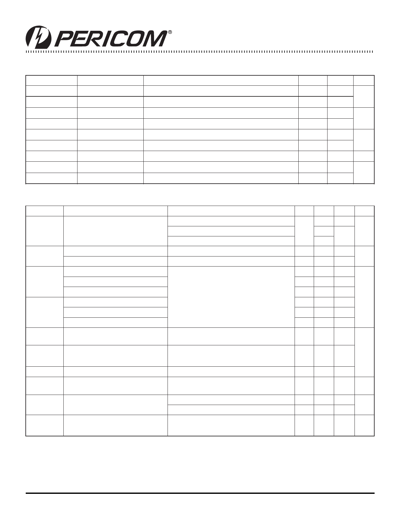
DC Electrical Characteristics for Commercial Temperature Devices
Parameter
VIL
VIH
IIL
IIH
Description
Input LOW Voltage
Input HIGH Voltage
Input LOW Current
Input HIGH Current
VIN = 0V
VIN = VDD
Test Conditions
¾
¾
Min. Max. Units
¾
0.8
2.0
¾
V
¾
¾
50
mA
100
VOL
Output LOW Voltage IOL = 8mA (1); IOL = 12mA (1H)
VOH
Output HIGH Voltage IOH = 8mA (1); IOH = 12mA (1H)
¾
0.4
2.4
¾
V
IDD (PI6C2309) Bypass, PLL off
SEL1 = 0 SEL2 = 1
¾
25 mA
IDD
Supply Current
Unloaded outputs, 66.67 MHz, Select inputs at VDD or GND
¾
39
mA
IDD
Supply Current
Unloaded outputs 100 MHz Select Inputs @ VDD or GND
¾
54
AC Electrical Characteristicsfor Commercial Temperature Device
Parame te rs
Name
Test Conditions
Min. Typ. Max. Units
30pF load (1, 1H)
100
FO
Output Frequency
tDC
tR
tF
tSK(O)
Duty Cycle(1) (1H)
Duty Cycle (1)
Rise Time(1) @30pF
Rise Time(1) @15pF
Rise Time(1) @30pF (1H)
Fall Time(1) @30pF
Fall Time(1) @15pF
Fall Time(1) @30pF (1H)
Output to Output Skew(1)
(1,1H)
20pF load, (1H)
15pF load, (1, 1H)
Measured at VDD/2, FO< 66MHz, 30pF
Measured at VDD/2, FO< 66MHz, 30pF
Measured between 0.8V and 2.0V
All outputs equally loaded, VDD/2
10
MHz
133
45 50 55
%
40 50 60
2.2
1.5
1.5
ns
2.2
1.5
1.25
200
t0
Input to Output Delay, CLKIN
Rising Edge to OUT0 Rising Edge(1)
Measured at VDD/2
0 ±350 ps
tSK(D)
tSLEW
tJIT
Device to Device Skew(1)
Output Slew Rate(1)
Cycle-to-Cycle Jitter(1) (1,1H)
tLOCK PLL Lock Time(1)
Measured at VDD/2 on OUT0 pins of devices
Measured between 0.8V and 2.0V on 1H
device using Test Circuit #2
1
Measured at 66.67 MHz, loaded 30pF outputs
Measured at 133 MHz, loaded 15pF outputs
Stable power supply, valid clocks
presented on CLKIN pins
0 600
V/ns
200
ps
100
1.0 ms
Notes:
1. See Switching Waveforms on page 6
5
PS8478B 10/30/01
Share Link: 