PI6C9930S Ver la hoja de datos (PDF) - Pericom Semiconductor
Número de pieza
componentes Descripción
Lista de partido
PI6C9930S Datasheet PDF : 5 Pages
| |||
PI6C9930 111222333444555666777888999000111222333444555666777888999000111222333444555666777888999000111222111222333444555666777888999000111222333444555666777888999000111222333444555666777888999000111222111222333444555666777888999000111222333444555666777888999000111222333444555666777888999000111222111222333444555666777888999000111222333444555666777888999000111222333444555666777888999000111222111222333444555666777888999000111222
3.3V Zero-Delay Clock Buffer
Features
• Near zero input to output delay
• Seven copies of the REF/2 or
Six copies of REF plus one REF × 2
• 25 100 MHz output
• 50% duty cycle
• Low skew
• Low jitter (<250ps cycle-to-cycle)
• Low noise balanced drive outputs
• VCC = 3.3V ±0.3V, TA = 0° to 70°
• 24-pin 209 mil wide SSOP (H)
• 24-pin 150 mil wide QSOP (Q)
• 24-pin 300 mil wide SOIC (S)
Applications
• PCI 66 MHz or 33 MHz systems
Product Description
The PI6C9930 Clock Buffer offers zero-delay, low-skew system
clock distribution. These multiple output clock drivers optimize the
timing of high-performance computer systems. Each of eight
individual drivers can drive series-terminated transmission lines
with impedances as low as 50Ω while delivering minimal output
skews and full-swing logic levels.
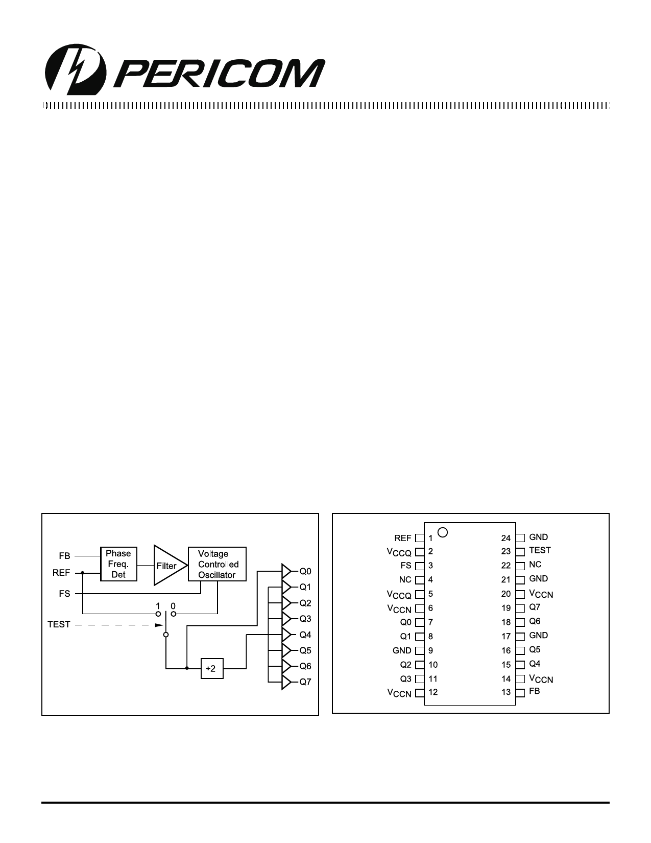
Connecting Q0 to FB provides REF/2 outputs on Q1-Q7. Connecting
any of Q1 - Q7 output to FB produces six copies of the REF input
plus one REF x 2 on Q0.
Test Mode
In normal system operation, this pin is connected to ground. For
testing purposes, the TEST pin can have a removable jumper to
ground, or be tied LOW through a 100Ω resistor. This will allow drive
by an external tester. If the TEST input is forced HIGH, the device
will operate with its internal phase-locked loop disconnected, and
input levels supplied to REF will directly control all outputs.
Relative output to output functions are the same as in normal mode.
Block Diagram
Pinout
24-Pin
H, Q, S
177
PS8096B 01/25/99
Share Link: 